SLLS447D October 2000 – April 2024 SN65LBC172A , SN75LBC172A
PRODUCTION DATA
- 1
- 1 Features
- 2 Applications
- 3 Description
- 4 Pin Configuration and Functions
- 5 Specifications
- 6 Parameter Measurement Information
- 7 Detailed Description
- 8 Application and Implementation
- 9 Device and Documentation Support
- 10Revision History
- 11Mechanical, Packaging, and Orderable Information
Package Options
Refer to the PDF data sheet for device specific package drawings
Mechanical Data (Package|Pins)
- DW|16
- N|16
- DW|20
Thermal pad, mechanical data (Package|Pins)
Orderable Information
3 Description
The SN65LBC172A and SN75LBC172A are quadruple differential line drivers with 3-state outputs, designed for TIA/EIA-485 (RS-485), TIA/EIA-422 (RS-422), and ISO 8482 applications.
These devices are optimized for balanced multipoint bus transmission at signaling rates up to 30 million bits per second. The transmission media may be printed-circuit board traces, backplanes, or cables. The ultimate rate and distance of data transfer is dependent upon the attenuation characteristics of the media and the noise coupling to the environment.
Each driver features current limiting and thermal-shutdown circuitry making it suitable for high-speed mulitpoint data transmission applications in noisy environments. These devices are designed using LinBiCMOS, facilitating low power consumption and robustness.
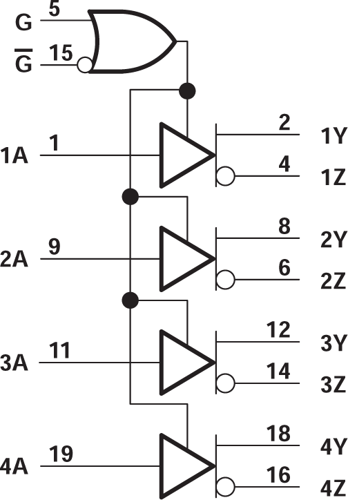
The G and G inputs provide driver enable control using either positive or negative logic. When disabled or powered off, the driver outputs present a high-impedance to the bus for reduced system loading.
The SN75LBC172A is characterized for operation over the temperature range of 0°C to 70°C. The SN65LBC172A is characterized over the temperature range from –40°C to 85°C.
| PART NUMBER | PACKAGE(1) | PACKAGE SIZE(2) |
|---|---|---|
| SN65LBC172A SN75LBC172A | SOIC (DW, 16) | 10.3mm × 10.3mm |
| SOIC (DW, 20) | 12.8mm × 10.3mm | |
| PDIP (N, 16) | 19.3mm × 9.4mm |
 Logic Diagram (Positive Logic)
 Logic Diagram (Positive Logic)