SLLS170F October 1993 – November 2023 SN65LBC173 , SN75LBC173
PRODUCTION DATA
- 1
- 1 Features
- 2 Applications
- 3 Description
- 4 Pin Configuration and Functions
- 5 Specifications
- 6 Parameter Measurement Information
- 7 Detailed Description
- 8 Device and Documentation Support
- 9 Revision History
- 10Mechanical, Packaging, and Orderable Information
Package Options
Mechanical Data (Package|Pins)
Thermal pad, mechanical data (Package|Pins)
Orderable Information
6 Parameter Measurement Information
 Figure 6-1 tpd and tt Test Circuit and Voltage Waveforms
A. The input pulse is supplied by a generator having the following characteristics: PRR = 1 MHz, duty cycle = 50%, tr ≤ 6 ns, tf ≤ 6 ns, ZO = 50 Ω.
B. CL includes probe and jig capacitance.
C. All diodes are 1N916 or equivalent.
D. To test the active-low enable G, ground G and apply an inverted input waveform to G.
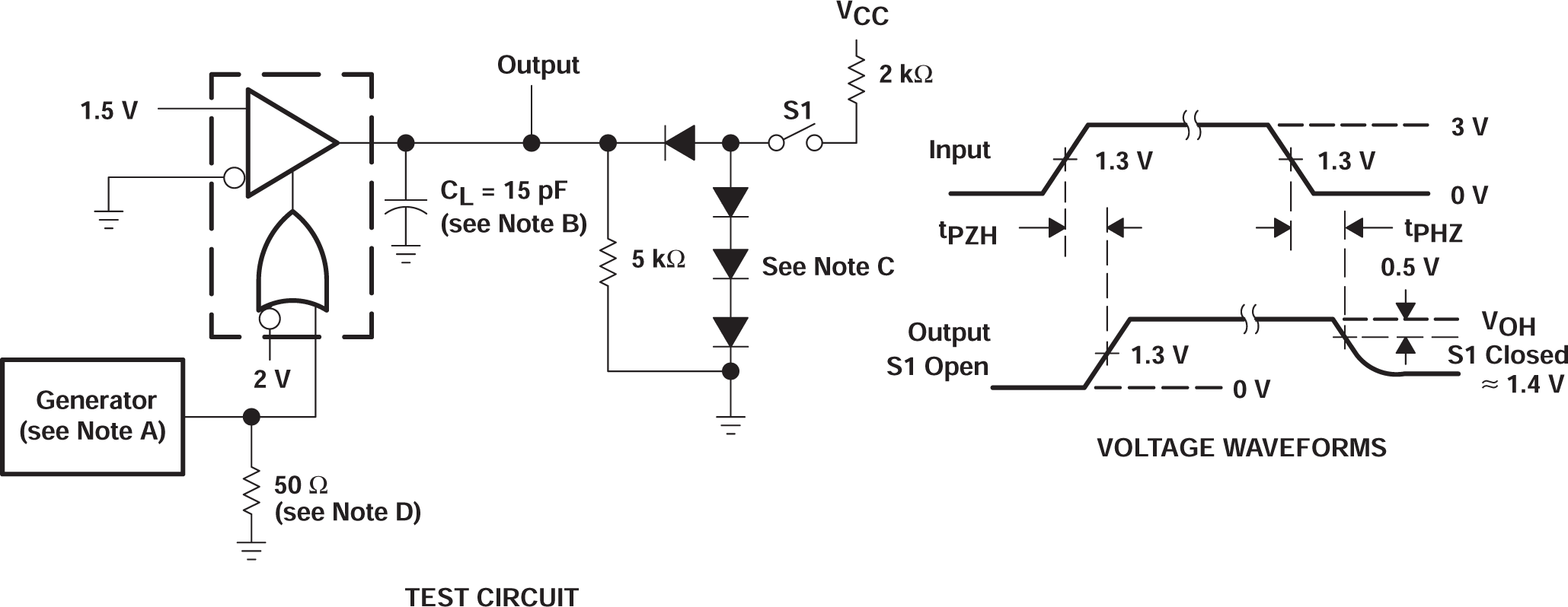
Figure 6-2 tPHZ and tPZH Test Circuit and Voltage Waveforms
A. The input pulse is supplied by a generator having the following characteristics: PRR = 1 MHz, duty cycle = 50%, tr ≤ 6 ns, tf ≤ 6 ns, ZO = 50 Ω.
B. CL includes probe and jig capacitance.
C. All diodes are 1N916 or equivalent.
D. To test the active-low enable G, ground G and apply an inverted input waveform to G.
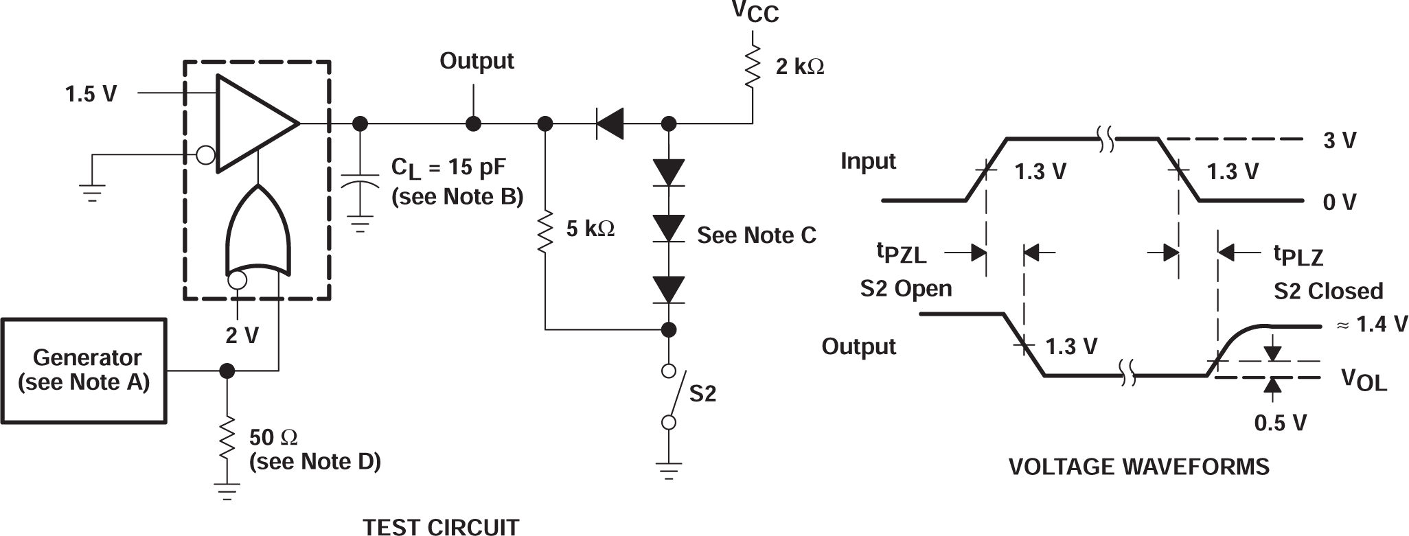
Figure 6-3 tPZL and tPLZ Test Circuit and Voltage Waveforms