SLLS170F October 1993 – November 2023 SN65LBC173 , SN75LBC173
PRODUCTION DATA
- 1
- 1 Features
- 2 Applications
- 3 Description
- 4 Pin Configuration and Functions
- 5 Specifications
- 6 Parameter Measurement Information
- 7 Detailed Description
- 8 Device and Documentation Support
- 9 Revision History
- 10Mechanical, Packaging, and Orderable Information
Package Options
Mechanical Data (Package|Pins)
Thermal pad, mechanical data (Package|Pins)
Orderable Information
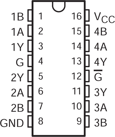
4 Pin Configuration and Functions
 Figure 4-1 D or N Package
(Top View)
Table 4-1 Pin Functions
| PIN | TYPE(1) | DESCRIPTION | |
|---|---|---|---|
| NAME | NO. | ||
| 1B | 1 | I | Channel 1 Inverting Differential Input |
| 1A | 2 | I | Channel 1 Non-Inverting Differential Input |
| 1Y | 3 | O | Channel 1 Output |
| G | 4 | I | Active High Receiver Enable |
| 2Y | 5 | O | Channel 2 Output |
| 2A | 6 | I | Channel 2 Non-Inverting Differential Input |
| 2B | 7 | I | Channel 2 Inverting Differential Input |
| GND | 8 | GND | Device Ground |
| 3B | 9 | I | Channel 3 Inverting Differential Input |
| 3A | 10 | I | Channel 3 Non-Inverting Differential Input |
| 3Y | 11 | O | Channel 3 Output |
| G | 12 | I | Active Low Receiver Enable |
| 4Y | 13 | O | Channel 4 Output |
| 4A | 14 | I | Channel 4 Non-Inverting Differential Input |
| 4B | 15 | I | Channel 4 Inverting Differential Input |
| VCC | 16 | POW | Device Supply |
(1) Signal Types: I = Input, O = Output, I/O = Input or Output.