SLLS455D November 2000 – November 2023 SN65LBC175A , SN75LBC175A
PRODUCTION DATA
- 1
- 1 Features
- 2 Applications
- 3 Description
- 4 Pin Configuration and Functions
- 5 Specifications
- 6 Parameter Measurement Information
- 7 Detailed Description
- 8 Application and Implementation
- 9 Device and Documentation Support
- 10Revision History
- 11Mechanical, Packaging, and Orderable Information
Package Options
Mechanical Data (Package|Pins)
Thermal pad, mechanical data (Package|Pins)
Orderable Information
5.8 Typical Characteristics
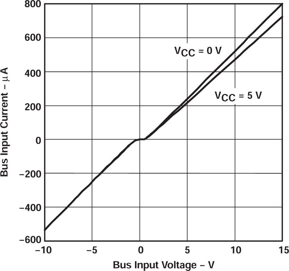 Figure 5-1 Bus Input Current vs Bus
Input Voltage
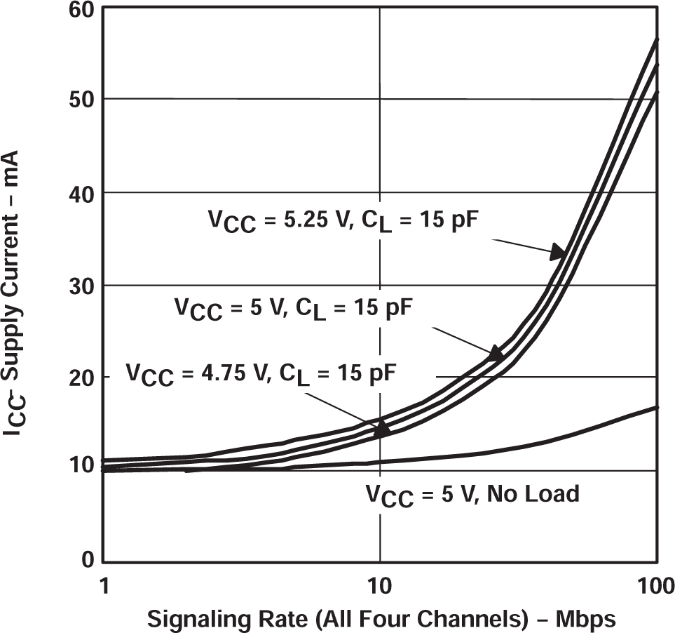 Figure 5-3 Supply Current vs
Signaling Rate (All Four Channels)
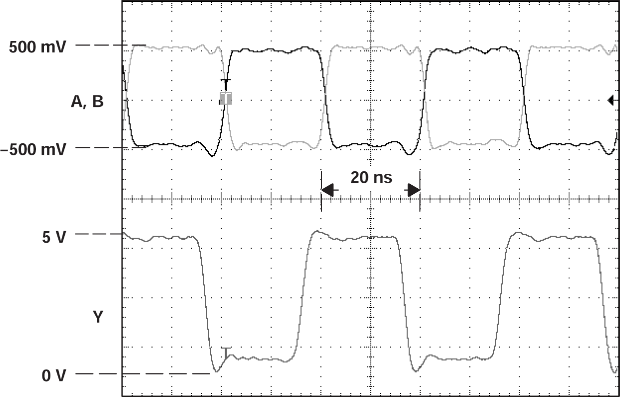 Figure 5-5 Receiver Inputs and
Outputs, 50 Mbps Signaling Rate
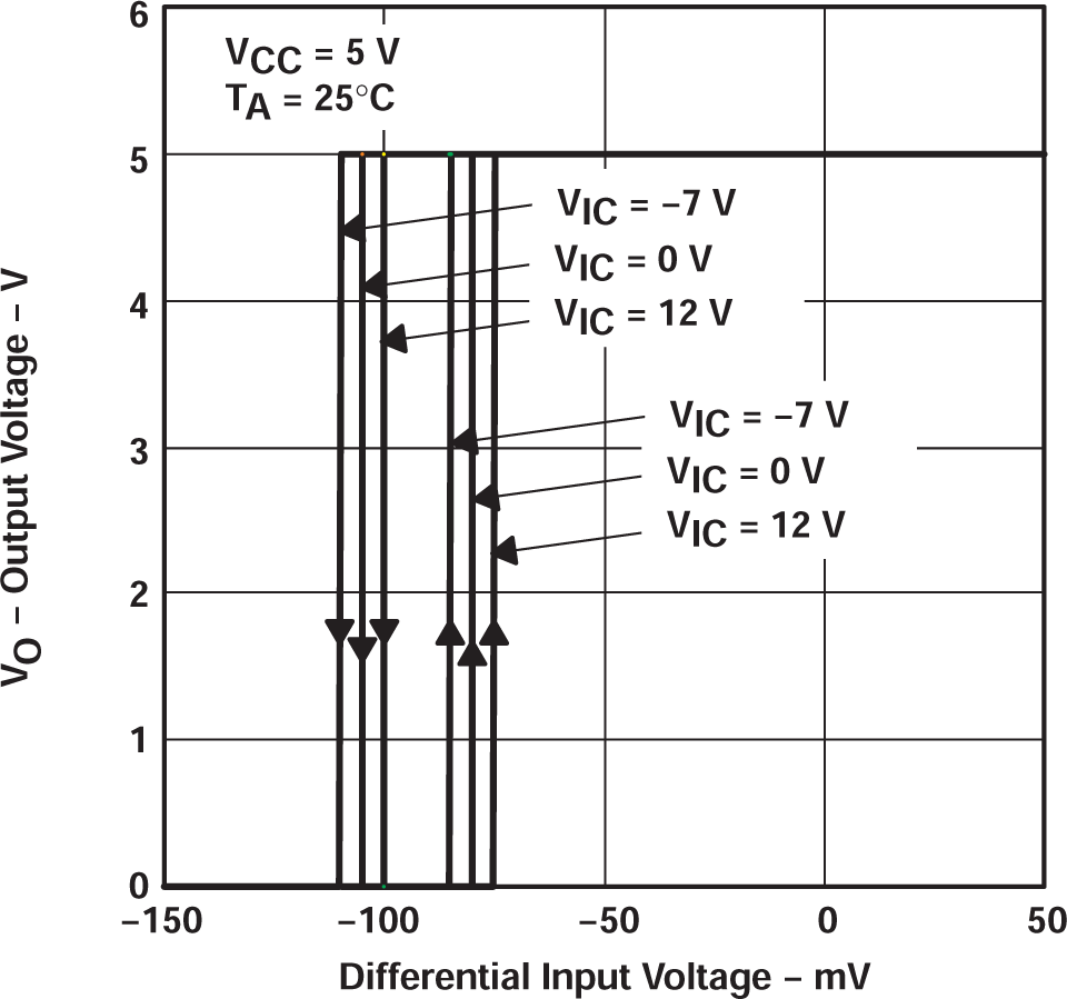 Figure 5-2 Output Voltage vs
Differential Input Voltage
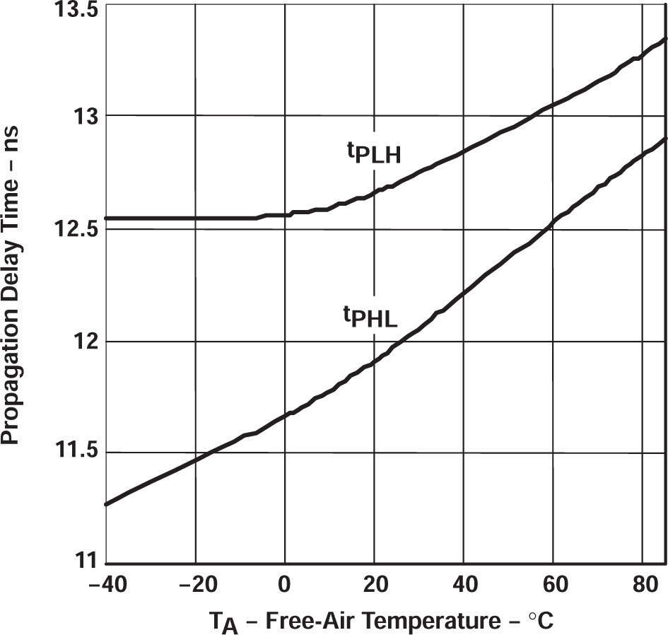 Figure 5-4 Propagation Delay Time vs
Free-air Temperature