SLLS455D November 2000 – November 2023 SN65LBC175A , SN75LBC175A
PRODUCTION DATA
- 1
- 1 Features
- 2 Applications
- 3 Description
- 4 Pin Configuration and Functions
- 5 Specifications
- 6 Parameter Measurement Information
- 7 Detailed Description
- 8 Application and Implementation
- 9 Device and Documentation Support
- 10Revision History
- 11Mechanical, Packaging, and Orderable Information
Package Options
Mechanical Data (Package|Pins)
Thermal pad, mechanical data (Package|Pins)
Orderable Information
7.1 Device Functional Modes
Table 7-1 Functional Table (Each
Receiver)
| DIFFERENTIAL INPUTS A – B (VID) | ENABLE EN(1) | OUTPUT Y |
|---|---|---|
| VID ≤ −0.2 V | H | L |
| −0.2 V < VID < −0.01 V | H | ? |
| −0.01 V ≤ VID | H | H |
| X | L | Z |
| X | OPEN | Z |
| Short circuit | H | H |
| Open circuit | H | H |
(1) H = high level, L = low level, X = irrelevant, Z =
high impedance (off), ? = indeterminate
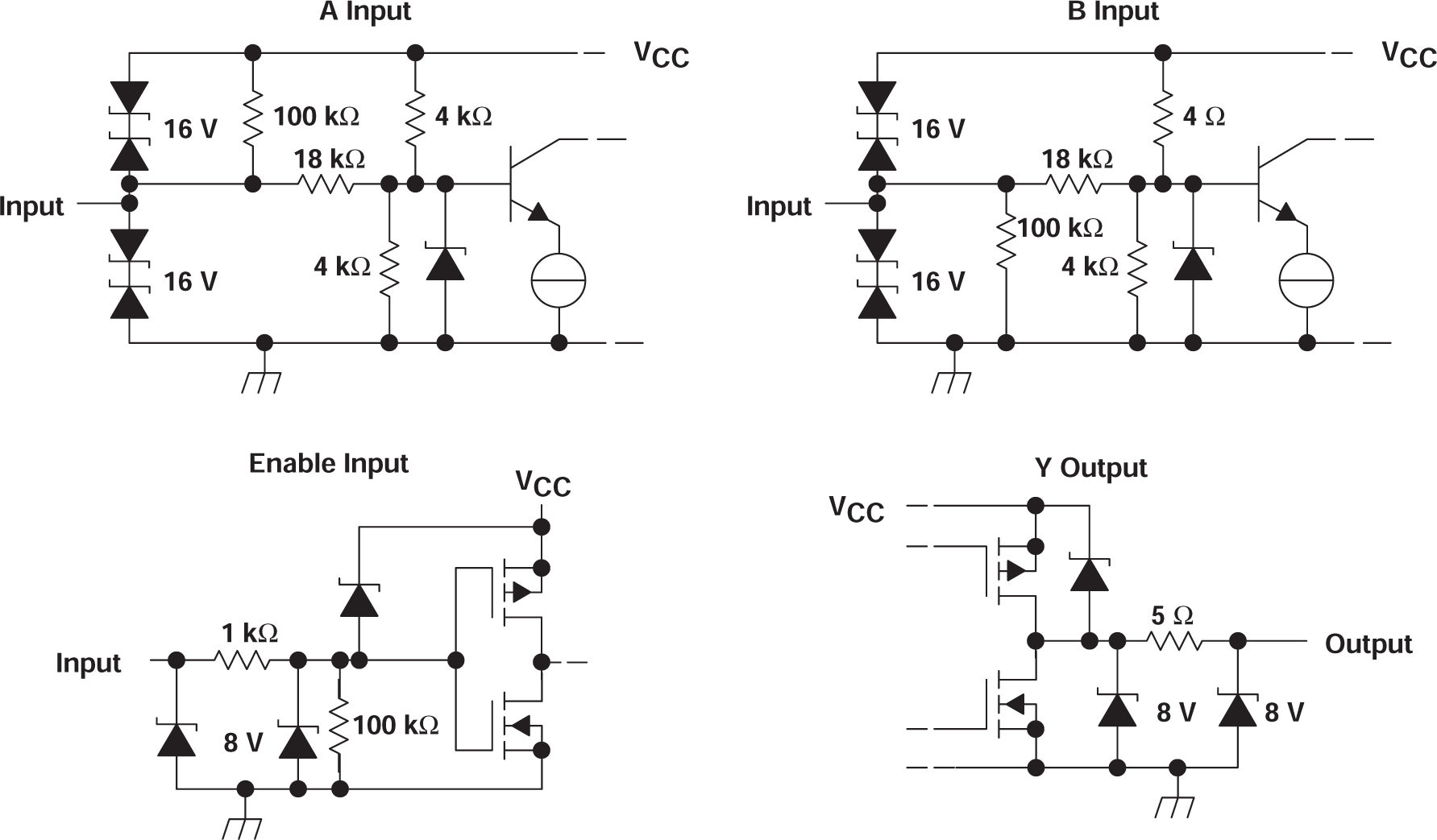
 Figure 7-1 Equivalent Input and Output
Schematic Diagrams