SGLS211B October 2003 – January 2023 SN65LBC176-Q1
PRODUCTION DATA
- 1Features
- 2Description
- 3Revision History
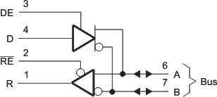
- 4Pin Configuration and Functions
- 5Specifications
- 6Detailed Description
- 7Device and Documentation Support
- 8Mechanical, Packaging, and Orderable Information
Package Options
Refer to the PDF data sheet for device specific package drawings
Mechanical Data (Package|Pins)
- D|8
Thermal pad, mechanical data (Package|Pins)
Orderable Information
2 Description
The SN65LBC176 differential bus transceiver is a monolithic, integrated circuit designed for bidirectional data communication on multipoint bus-transmission lines. It is designed for balanced transmission lines and meets ANSI Standard RS-485 and ISO 8482:1987(E).
The SN65LBC176 combines a 3-state, differential line driver and a differential input line receiver, both of which operate from a single 5-V power supply. The driver and receiver have active-high and active-low enables, respectively, which can externally connect together to function as a direction control. The driver differential outputs and the receiver differential inputs connect internally to form a differential input/output (I/O) bus port that is designed to offer minimum loading to the bus whenever the driver is disabled or VCC = 0. This port features wide positive and negative common-mode voltage ranges, making the device suitable for party-line applications. Very low device supply current can be achieved by disabling the driver and the receiver. Both the driver and receiver are available as cells in the Texas Instruments LinASIC Library.
This transceiver is suitable for ANSI Standard RS-485 and ISO 8482:1987 (E) applications to the extent that they are specified in the operating conditions and characteristics section of this data sheet. Certain limits contained in the ANSI Standard RS-485 and ISO 8482:1987 (E) are not met or cannot be tested over the entire extended temperature range.
| PART NUMBER | PACKAGE(1) | BODY SIZE (NOM) |
|---|---|---|
| SN65LBC176-Q1 | D (SOIC) (8) | 4.90 mm x 3.91 mm |