SLLS173G January 1994 – October 2022 SN65LBC179 , SN75LBC179
PRODUCTION DATA
- 1Features
- 2Description
- 3Revision History
- 4Pin Configuration and Functions
-
5Specifications
- 5.1 Absolute Maximum Ratings
- 5.2 Recommended Operating Conditions
- 5.3 Thermal Information
- 5.4 Dissipation Rating Table
- 5.5 Electrical Characteristics - Driver
- 5.6 Switching Characteristics - Driver
- 5.7 Electrical Characteristics - Receiver
- 5.8 Switching Characteristics - Receiver
- 5.9 Typical Characteristics
- 6Parameter Measurement Information
- 7Detailed Description
- 8Device and Documentation Support
- 9Mechanical, Packaging, and Orderable Information
Package Options
Mechanical Data (Package|Pins)
Thermal pad, mechanical data (Package|Pins)
Orderable Information
6 Parameter Measurement Information
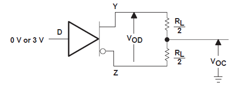
 Figure 6-1 Differential and Common-Mode
Output Voltage Test Circuit
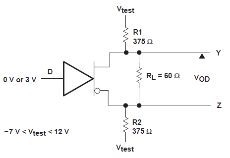
 Figure 6-2 Differential Output Voltage
Test Circuit
A. The
input pulse is supplied by a generator having the following characteristics: PRR
≤ 1 MHz, 50% duty cycle, tr ≤ 6 ns, tf≤ 6 ns,
ZO = 50 Ω.
B. CL includes probe and jig capacitance.
Figure 6-3 Driver Test Circuits and
Differential Output Delay and Transition Time Voltage Waveforms
A. The
input pulse is supplied by a generator having the following characteristics: PRR
≤ 1 MHz, 50% duty cycle, tr ≤ 6 ns, tf≤ 6 ns,
ZO = 50 Ω.
B. CL includes probe and jig capacitance.
Figure 6-4 Receiver Test Circuit and
Propagation Delay and Transition Time Voltage Waveforms