SLLS173G January 1994 – October 2022 SN65LBC179 , SN75LBC179
PRODUCTION DATA
- 1Features
- 2Description
- 3Revision History
- 4Pin Configuration and Functions
-
5Specifications
- 5.1 Absolute Maximum Ratings
- 5.2 Recommended Operating Conditions
- 5.3 Thermal Information
- 5.4 Dissipation Rating Table
- 5.5 Electrical Characteristics - Driver
- 5.6 Switching Characteristics - Driver
- 5.7 Electrical Characteristics - Receiver
- 5.8 Switching Characteristics - Receiver
- 5.9 Typical Characteristics
- 6Parameter Measurement Information
- 7Detailed Description
- 8Device and Documentation Support
- 9Mechanical, Packaging, and Orderable Information
Package Options
Mechanical Data (Package|Pins)
Thermal pad, mechanical data (Package|Pins)
Orderable Information
5.9 Typical Characteristics
 Figure 5-1 Driver High-Level Output Voltage vs High-Level Output Current
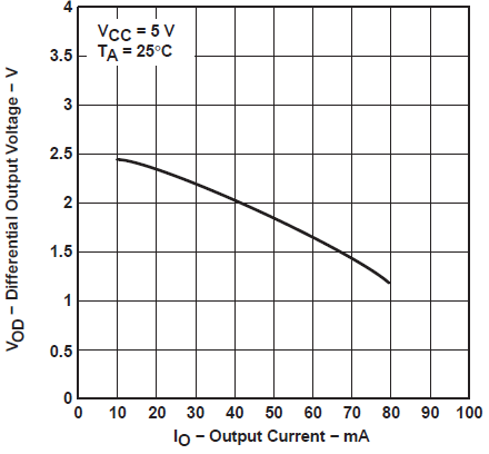 Figure 5-3 Driver Differential Output Voltage vs Output Current
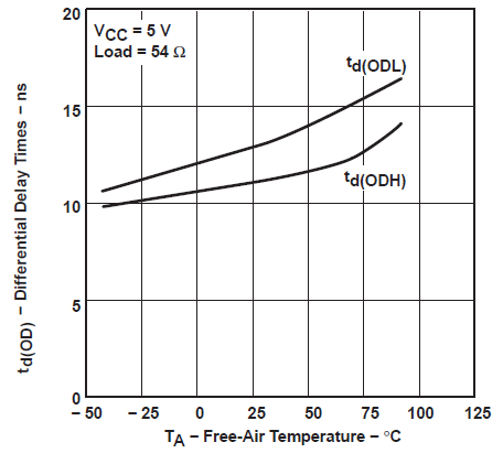 Figure 5-5 Driver Differential Delay Time vs Free-Air Temperature
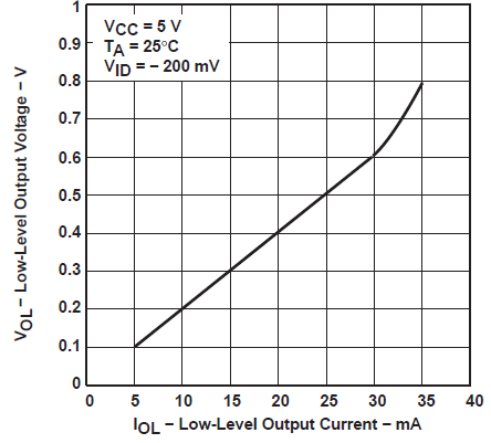 Figure 5-7 Receiver Low-Level Output
Voltage vs Low-Level Output Current
 Figure 5-9 Average Supply Current vs
Frequency
 Figure 5-11 Receiver Propagation Delay
Time vs Free-Air Temperature
 Figure 5-2 Driver Low-Level Output Voltage vs Low-Level Output Current
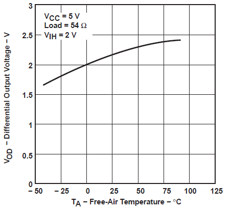 Figure 5-4 Driver Differential Output Voltage vs Free-Air Temperature
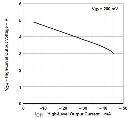 Figure 5-6 Receiver High-Level Output Voltage vs High-Level Output Current
 Figure 5-8 Receiver Output Voltage vs
Differential Input Voltage
 Figure 5-10 Receiver Input Current vs
Input Voltage (Complementary Input at 0 V)