SLLS236J October 1996 – July 2024 SN65LBC184 , SN75LBC184
PRODUCTION DATA
- 1
- 1 Features
- 2 Applications
- 3 Description
- 4 Pin Configuration and Functions
-
5 Specifications
- 5.1 Absolute Maximum Ratings
- 5.2 ESD Ratings
- 5.3 Recommended Operating Conditions
- 5.4 Thermal Information
- 5.5 Electrical Characteristics: Driver
- 5.6 Electrical Characteristics: Receiver
- 5.7 Driver Switching Characteristics
- 5.8 Receiver Switching Characteristics
- 5.9 Dissipation Ratings
- 5.10 Typical Characteristics
- 6 Parameter Measurement Information
- 7 Detailed Description
- 8 Application and Implementation
- 9 Device and Documentation Support
- 10Revision History
- 11Mechanical, Packaging, and Orderable Information
Package Options
Mechanical Data (Package|Pins)
Thermal pad, mechanical data (Package|Pins)
Orderable Information
3 Description
The SN75LBC184 and SN65LBC184 devices are differential data line transceivers in the trade-standard footprint of the SN75176 with built-in protection against high-energy noise transients. This feature provides a substantial increase in reliability for better immunity to noise transients coupled to the data cable over most existing devices. Use of these circuits provides a reliable low-cost direct-coupled (with no isolation transformer) data line interface without requiring any external components.
The SN75LBC184 and SN65LBC184 can withstand overvoltage transients of 400W peak (typical). The conventional combination wave called out in IEC 61000-4-5 simulates the overvoltage transient and models a unidirectional surge caused by overvoltages from switching and secondary lightning transients.
| PART NUMBER | PACKAGE(1) | PACKAGE SIZE(2) |
|---|---|---|
| SN65LBC184, SN75LBC184 |
SOIC (8) | 4.9mm × 6mm |
| PDIP (8) | 9.81mm × 6.35mm |
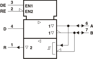
 Logic Symbol(1)