SLLS236J October 1996 – July 2024 SN65LBC184 , SN75LBC184
PRODUCTION DATA
- 1
- 1 Features
- 2 Applications
- 3 Description
- 4 Pin Configuration and Functions
-
5 Specifications
- 5.1 Absolute Maximum Ratings
- 5.2 ESD Ratings
- 5.3 Recommended Operating Conditions
- 5.4 Thermal Information
- 5.5 Electrical Characteristics: Driver
- 5.6 Electrical Characteristics: Receiver
- 5.7 Driver Switching Characteristics
- 5.8 Receiver Switching Characteristics
- 5.9 Dissipation Ratings
- 5.10 Typical Characteristics
- 6 Parameter Measurement Information
- 7 Detailed Description
- 8 Application and Implementation
- 9 Device and Documentation Support
- 10Revision History
- 11Mechanical, Packaging, and Orderable Information
Package Options
Mechanical Data (Package|Pins)
Thermal pad, mechanical data (Package|Pins)
Orderable Information
7.4 Device Functional Modes
When the driver enable pin (DE) is logic high, the differential outputs A and B follow the logic states at data input D. A logic high at D causes A to turn high and B to turn low. In this case, the differential output voltage defined as VOD = VA – VB is positive. When D is low, the output states reverse, B turns high, A becomes low, and VOD is negative.
When DE is low, both outputs turn high-impedance. In this condition, the logic state at D is irrelevant.
| INPUT(1) | ENABLE | OUTPUTS | FUNCTION | |
|---|---|---|---|---|
| D | DE | A | B | |
| H | H | H | L | Actively drive bus High |
| L | H | L | H | Actively drive bus Low |
| X | L | Z | Z | Driver disabled |
When the receiver enable pin, RE, is logic low, the receiver is enabled. When the differential input voltage defined as VID = VA – VB is positive and higher than the positive input threshold, VIT+, the receiver output (R) turns high. When VID is negative and lower than the negative input threshold, VIT–, the receiver output turns low. If VID is between VIT+ and VIT–, the output is indeterminate.
When RE is logic high, the receiver output is high-impedance and the magnitude and polarity of VID are irrelevant. When the transceiver is disconnected from the bus, the receiver provides a failsafe high output.
| DIFFERENTIAL INPUT | ENABLE(1) | OUTPUT | FUNCTION |
|---|---|---|---|
| VID = VA – VB | RE | R | |
| VID > VIT+ | L | H | Receive valid bus High |
| VIT– < VID < VIT+ | L | ? | Indeterminate bus state |
| VID < VIT– | L | L | Receive valid bus Low |
| X | H | Z | Receiver disabled |
| OPEN | L | H | Receiver failsafe High |
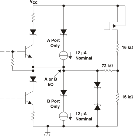
 Figure 7-2 Schematic of Inputs and Outputs