SLLSEA8A January 2012 – March 2016 SN65LVCP114
PRODUCTION DATA.
- 1 Features
- 2 Applications
- 3 Description
- 4 Revision History
- 5 Description (continued)
- 6 Pin Configuration and Functions
- 7 Specifications
- 8 Parameter Measurement Information
-
9 Detailed Description
- 9.1 Overview
- 9.2 Functional Block Diagram
- 9.3 Feature Description
- 9.4 Device Functional Modes
- 9.5 Programming
- 9.6
Register Maps
- 9.6.1
SN65LVCP114 Register Mapping Information
- 9.6.1.1 Register 0x00
- 9.6.1.2 Register 0x01
- 9.6.1.3 Register 0x02
- 9.6.1.4 Register 0x03
- 9.6.1.5 Register 0x04
- 9.6.1.6 Register 0x06
- 9.6.1.7 Register 0x07
- 9.6.1.8 Register 0x08
- 9.6.1.9 Register 0x0A
- 9.6.1.10 Register 0x0B
- 9.6.1.11 Register 0x0C
- 9.6.1.12 Register 0x0D
- 9.6.1.13 Register 0x0F
- 9.6.1.14 Register 0x10
- 9.6.1.15 Register 0x11
- 9.6.1.16 Register 0x12
- 9.6.1.17 Register Descriptions
- 9.6.1
SN65LVCP114 Register Mapping Information
- 10Application and Implementation
- 11Power Supply Recommendations
- 12Layout
- 13Device and Documentation Support
- 14Mechanical, Packaging, and Orderable Information
Package Options
Mechanical Data (Package|Pins)
- ZJA|167
Thermal pad, mechanical data (Package|Pins)
Orderable Information
10 Application and Implementation
NOTE
Information in the following applications sections is not part of the TI component specification, and TI does not warrant its accuracy or completeness. TI’s customers are responsible for determining suitability of components for their purposes. Customers should validate and test their design implementation to confirm system functionality.
10.1 Application Information
The SN65LVCP114 device has enough equalization to be placed on the receiver side and compensate traces up to 24 inches. The SN65LVCP114 device can be placed on transmitter side and still have an open eye after a trace of 24 inches.
10.2 Typical Applications
10.2.1 Transmit-Side Typical Application
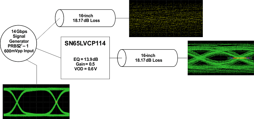 Figure 34. Transmit-Side Typical Application
10.2.1.1 Design Requirements
Table 17 lists the design parameters of the SN65LVCP114.
Table 17. Design Parameters
| DESIGN PARAMETER | EXAMPLE VALUE |
|---|---|
| VCC | 3.3 V |
| VOD | 600 mV |
| EQ | 13.9 dB |
| GAIN | 0.5 (–6 dB) |
| Trace length | 16 inches |
10.2.1.2 Detailed Design Procedure
- Determine the loss profile between transmitter and receiver.
- Based upon loss profile and signal swing, determine the optimal equalization settings.
- Select appropriate voltage output swing.
- If required select correct differential pair polarity.
- To set voltage logic levels on configuration pins, use a 5-kΩ pullup for high level, tie pin to GND for low level, and place a 5-kΩ pullup and 5-kΩ pulldown for HiZ.
10.2.1.3 Application Curves
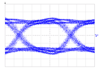 Figure 35. Input to SN65LVCP114
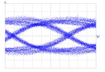 Figure 36. Output to SN65LVCP114 After Trace
10.2.2 Receive-Side Typical Application
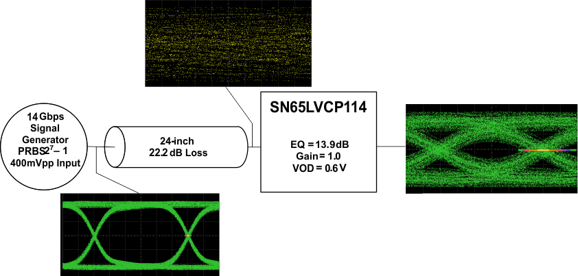 Figure 37. Receive-Side Typical Application
10.2.2.1 Design Requirements
Table 18 lists the design parameters of the SN65LVCP114.
Table 18. Design Parameters
| DESIGN PARAMETER | EXAMPLE VALUE |
|---|---|
| VCC | 3.3 V |
| VOD | 600 mV |
| EQ | 13.9 dB |
| Gain | 1 (0 dB) |
| Trace lenght | 24 inches |
10.2.2.2 Detailed Design Procedure
- Determine the loss profile between transmitter and receiver.
- Based upon the loss profile and signal swing, determine the optimal equalization settings.
- Select appropriate voltage output swing.
- If required, select the correct differential pair polarity.
- To set voltage logic levels on configuration pins, use a 5-kΩ pullup for high level, tie pin to GND for low level, and place a 5-kΩ pullup and 5-kΩ pulldown for HiZ.
10.2.2.3 Application Curves
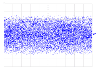 Figure 38. Input to SN65LVCP114
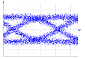 Figure 39. Output to SN65LVCP114 After Trace