SLLS575A AUGUST 2003 – July 2015 SN65LVDS049
PRODUCTION DATA.
- 1 Features
- 2 Applications
- 3 Description
- 4 Revision History
- 5 Pin Configuration and Functions
- 6 Specifications
- 7 Parameter Measurement Information
- 8 Detailed Description
-
9 Application and Implementation
- 9.1 Application Information
- 9.2
Typical Applications
- 9.2.1
Point-to-Point Communications
- 9.2.1.1 Design Requirements
- 9.2.1.2
Detailed Design Procedure
- 9.2.1.2.1 Bypass Capacitance
- 9.2.1.2.2 Driver Supply Voltage
- 9.2.1.2.3 Driver Input Voltage
- 9.2.1.2.4 Driver Output Voltage
- 9.2.1.2.5 Interconnecting Media
- 9.2.1.2.6 PCB Transmission Lines
- 9.2.1.2.7 Termination Resistor
- 9.2.1.2.8 Receiver Supply Voltage
- 9.2.1.2.9 Receiver Input Common-Mode Range
- 9.2.1.2.10 Receiver Input Signal
- 9.2.1.2.11 Receiver Output Signal
- 9.2.1.3 Application Curve
- 9.2.2 Multidrop Communications
- 9.2.1
Point-to-Point Communications
- 10Power Supply Recommendations
- 11Layout
- 12Device and Documentation Support
- 13Mechanical, Packaging, and Orderable Information
Package Options
Mechanical Data (Package|Pins)
- PW|16
Thermal pad, mechanical data (Package|Pins)
Orderable Information
1 Features
- DS90LV049 Compatible
- Up to 400-Mbps Signaling Rates
- Flow-Through Pinout
- 50-ps Driver Channel-to-Channel Skew (Typical)
- 50-ps Receiver Channel-to-Channel Skew (Typical)
- 3.3-V Power Supply
- High-Impedance Disable for All Outputs
- Internal Fail-safe Biasing of Receiver Inputs
- 1.4-ns Driver Propagation Delay (Typical)
- 1.9-ns Receiver Propagation Delay (Typical)
- High-Impedance Bus Pins on Power Down
- ANSI TIA/EIA-644-A Compliant
- Receiver Input and Driver Output ESD Exceeds 10 kV
- 16-Pin TSSOP Package
2 Applications
- Full-Duplex LVDS Communications of Clock and Data
- Printers
3 Description
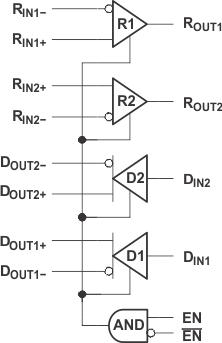
The SN65LVDS049 device is a dual flow-through differential line driver-receiver pair that uses low-voltage differential signaling (LVDS) to achieve signaling rates as high as 400 Mbps. The driver and receiver electrical interfaces are compliant to the TIA/EIA-644-A standard.
The intended application of this device and signaling technique is for point-to-point baseband data transmission over controlled impedance media of approximately 100-Ω characteristic impedance. The transmission media may be printed-circuit board traces, backplanes, or cables. The ultimate rate and distance of data transfer is dependent upon the attenuation characteristics of the media, the noise coupling to the environment, and other application specific characteristics.
The SN65LVDS049 is characterized for operation from –40°C to 85°C
Device Information(1)
| PART NUMBER | PACKAGE | BODY SIZE (NOM) |
|---|---|---|
| SN65LVDS049 | TSSOP (16) | 5.00 mm × 4.40 mm |
- For all available packages, see the orderable addendum at the end of the data sheet.
Block Diagram
