SLLS575A AUGUST 2003 – July 2015 SN65LVDS049
PRODUCTION DATA.
- 1 Features
- 2 Applications
- 3 Description
- 4 Revision History
- 5 Pin Configuration and Functions
- 6 Specifications
- 7 Parameter Measurement Information
- 8 Detailed Description
-
9 Application and Implementation
- 9.1 Application Information
- 9.2
Typical Applications
- 9.2.1
Point-to-Point Communications
- 9.2.1.1 Design Requirements
- 9.2.1.2
Detailed Design Procedure
- 9.2.1.2.1 Bypass Capacitance
- 9.2.1.2.2 Driver Supply Voltage
- 9.2.1.2.3 Driver Input Voltage
- 9.2.1.2.4 Driver Output Voltage
- 9.2.1.2.5 Interconnecting Media
- 9.2.1.2.6 PCB Transmission Lines
- 9.2.1.2.7 Termination Resistor
- 9.2.1.2.8 Receiver Supply Voltage
- 9.2.1.2.9 Receiver Input Common-Mode Range
- 9.2.1.2.10 Receiver Input Signal
- 9.2.1.2.11 Receiver Output Signal
- 9.2.1.3 Application Curve
- 9.2.2 Multidrop Communications
- 9.2.1
Point-to-Point Communications
- 10Power Supply Recommendations
- 11Layout
- 12Device and Documentation Support
- 13Mechanical, Packaging, and Orderable Information
Package Options
Mechanical Data (Package|Pins)
- PW|16
Thermal pad, mechanical data (Package|Pins)
Orderable Information
8 Detailed Description
8.1 Overview
The SN65LVDS049 device is a dual flow-through differential line driver-receiver pair that uses low-voltage differential signaling (LVDS) to achieve signaling rates of up to 400 Mbps. The device operates from a single supply that is nominally 3.3 V, but can be as low as 3.0 V and as high as 3.6 V. The TIA/EIA-644-A standard compliant electrical interface provides a minimum differential output voltage magnitude of 250 mV into a 100-Ω load and receipt of signals with up to 1 V of ground potential difference between a transmitter and receiver. The LVDS receivers have internal fail-safe biasing that places the outputs into a known high state for unconnected differential inputs.
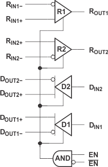
8.2 Functional Block Diagram

8.3 Feature Description
8.3.1 Driver Offset
An LVDS-compliant driver is required to maintain the common-mode output voltage at 1.2 V. The SN65LVDS049 incorporates sense circuitry and a control loop to source common-mode current and keep the output signal within specified values. Further, the device maintains the output common-mode voltage at this set point over the full 3 V to 3.6 V supply range.
8.3.2 Receiver Open Circuit Fail-Safe
One of the most common problems with differential signaling applications is how the system responds when no differential voltage is present on the signal pair. The LVDS receiver is like most differential line receivers in that its output logic state can be indeterminate when the differential input voltage is in the range from –100 mV to 100 mV and within its recommended input common-mode voltage range. However, the TI LVDS receiver is different in how it handles the open-input circuit situation.
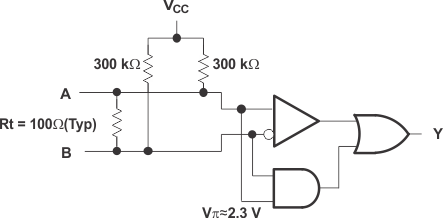
Open circuit means that there is little or no input current to the receiver from the data line itself. This could be when the driver is in a high-impedance state or the cable is disconnected. When this occurs, the LVDS receiver pulls each line of the signal to VCC through 300-kΩ resistors as shown in Figure 6. The fail-safe feature uses an AND gate to detect this condition and force the output to a high level.
 Figure 6. Open-Circuit Fail-Safe of the LVDS Receiver
Only under these conditions is the output of the receiver valid with less than a 100-mV differential input voltage magnitude. The presence of the termination resistor, Rt, does not affect the fail-safe function as long as it is connected as shown in Figure 6. Other termination circuits may allow a DC to ground that could defeat the pullup currents from the receiver and the fail-safe feature.
8.3.3 Receiver Common-Mode Range
For all supply voltages, the valid input signal is from ground to 0.9 V below the supply rail. Hence, if the device is operating with a 3.3-V supply, and a minimum differential voltage of 100 mV, common-mode values in the range of 0.05 V to 2.35 V are supported.
8.4 Device Functional Modes
Table 1. Driver Truth Table
| INPUT | ENABLES | OUTPUTS(1) | ||
|---|---|---|---|---|
| DIN | EN | EN | DOUT+ | DOUT– |
| L | H | L or OPEN | L | H |
| H | H | L | ||
| X | All other conditions | Z | Z | |
Table 2. Receiver Truth Table
| DIFFERENTIAL INPUT | ENABLES | OUTPUT(1) | |
|---|---|---|---|
| RIN- - RIN+ | EN | EN | ROUT |
| VID ≥ 100 mV | H | L or OPEN | H |
| VID ≤ - 100 mV | L | ||
| Open/short or terminated | H | ||
| X | All other conditions | Z | |
Table 3. Enable Function Table
| ENABLES | OUTPUTS | ||
|---|---|---|---|
| EN | EN | LVDS Out | LVCMOS Out |
| L or Open | L or Open | Disabled | Disabled |
| H | L or Open | Enabled | Enabled |
| L or Open | H | Disabled | Disabled |
| H | H | Disabled | Disabled |
 Figure 7. Equivalent Input and Output Schematic Diagrams
 Figure 8. Equivalent Input and Output Schematic Diagrams