SLLS575A AUGUST 2003 – July 2015 SN65LVDS049
PRODUCTION DATA.
- 1 Features
- 2 Applications
- 3 Description
- 4 Revision History
- 5 Pin Configuration and Functions
- 6 Specifications
- 7 Parameter Measurement Information
- 8 Detailed Description
-
9 Application and Implementation
- 9.1 Application Information
- 9.2
Typical Applications
- 9.2.1
Point-to-Point Communications
- 9.2.1.1 Design Requirements
- 9.2.1.2
Detailed Design Procedure
- 9.2.1.2.1 Bypass Capacitance
- 9.2.1.2.2 Driver Supply Voltage
- 9.2.1.2.3 Driver Input Voltage
- 9.2.1.2.4 Driver Output Voltage
- 9.2.1.2.5 Interconnecting Media
- 9.2.1.2.6 PCB Transmission Lines
- 9.2.1.2.7 Termination Resistor
- 9.2.1.2.8 Receiver Supply Voltage
- 9.2.1.2.9 Receiver Input Common-Mode Range
- 9.2.1.2.10 Receiver Input Signal
- 9.2.1.2.11 Receiver Output Signal
- 9.2.1.3 Application Curve
- 9.2.2 Multidrop Communications
- 9.2.1
Point-to-Point Communications
- 10Power Supply Recommendations
- 11Layout
- 12Device and Documentation Support
- 13Mechanical, Packaging, and Orderable Information
Package Options
Mechanical Data (Package|Pins)
- PW|16
Thermal pad, mechanical data (Package|Pins)
Orderable Information
7 Parameter Measurement Information
 Figure 1. Driver VOD and VOS Test Circuit
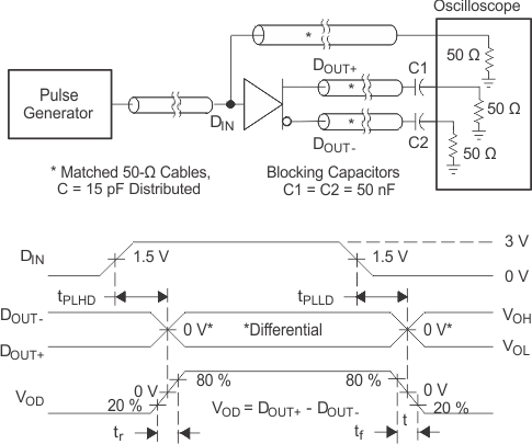
 Figure 2. Driver Propagation Delay and Rise and Fall Time Test Circuit and Waveforms
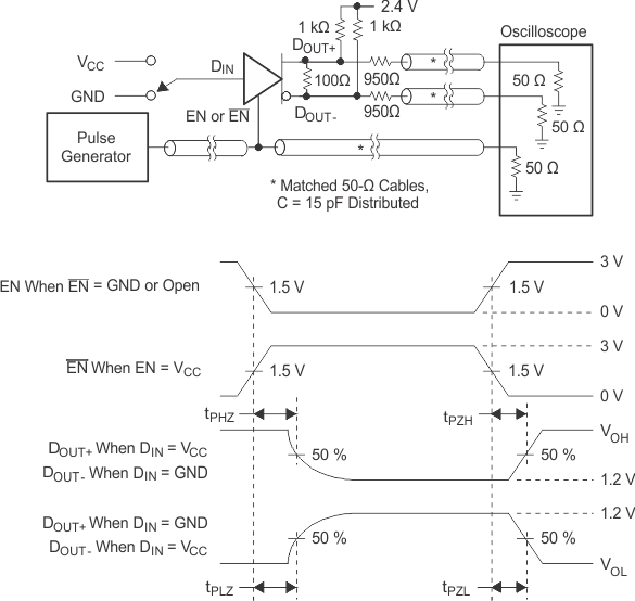
 Figure 3. Driver High-Impedance State Delay Test Circuit and Waveforms
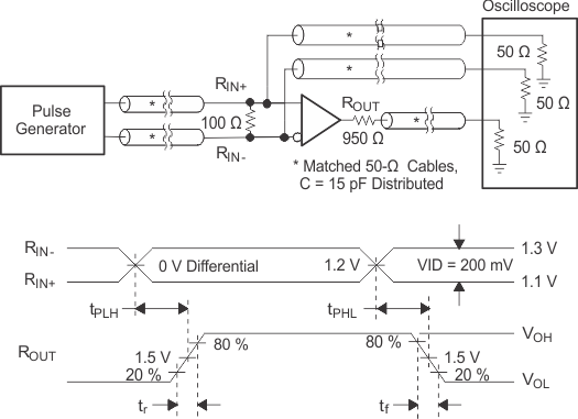
 Figure 4. Receiver Propagation Delay and Rise and Fall Test Circuit and Waveforms
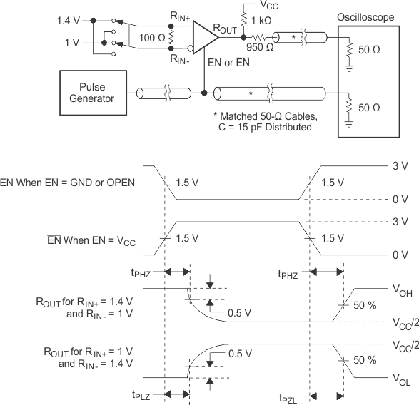
 Figure 5. Receiver High-Impedance State Delay Test Circuit and Waveforms
 (VCC = 3.3 V)