SLLS575A AUGUST 2003 – July 2015 SN65LVDS049
PRODUCTION DATA.
- 1 Features
- 2 Applications
- 3 Description
- 4 Revision History
- 5 Pin Configuration and Functions
- 6 Specifications
- 7 Parameter Measurement Information
- 8 Detailed Description
-
9 Application and Implementation
- 9.1 Application Information
- 9.2
Typical Applications
- 9.2.1
Point-to-Point Communications
- 9.2.1.1 Design Requirements
- 9.2.1.2
Detailed Design Procedure
- 9.2.1.2.1 Bypass Capacitance
- 9.2.1.2.2 Driver Supply Voltage
- 9.2.1.2.3 Driver Input Voltage
- 9.2.1.2.4 Driver Output Voltage
- 9.2.1.2.5 Interconnecting Media
- 9.2.1.2.6 PCB Transmission Lines
- 9.2.1.2.7 Termination Resistor
- 9.2.1.2.8 Receiver Supply Voltage
- 9.2.1.2.9 Receiver Input Common-Mode Range
- 9.2.1.2.10 Receiver Input Signal
- 9.2.1.2.11 Receiver Output Signal
- 9.2.1.3 Application Curve
- 9.2.2 Multidrop Communications
- 9.2.1
Point-to-Point Communications
- 10Power Supply Recommendations
- 11Layout
- 12Device and Documentation Support
- 13Mechanical, Packaging, and Orderable Information
Package Options
Mechanical Data (Package|Pins)
- PW|16
Thermal pad, mechanical data (Package|Pins)
Orderable Information
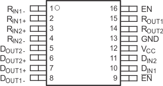
5 Pin Configuration and Functions
PW Package (Marked as LVDS049)
16-Pin TSSOP
(Top View)

Pin Functions
| PIN | I/O | DESCRIPTION | |
|---|---|---|---|
| NAME | NO. | ||
| GND | 13 | – | Ground |
| DIN1 | 10 | I | LVTTL input signals |
| DIN2 | 11 | ||
| DOUT1+ | 7 | O | Differential (LVDS) noninverting output |
| DOUT2+ | 6 | ||
| DOUT1– | 8 | O | Differential (LVDS) inverting output |
| DOUT2– | 5 | ||
| EN | 16 | I | Driver and receiver enable |
| EN | 9 | I | Driver and receiver inverse-enable |
| RIN1+ | 2 | I | Differential (LVDS) noninverting input |
| RIN2+ | 3 | ||
| RIN1– | 1 | I | Differential (LVDS) inverting input |
| RIN2– | 4 | ||
| ROUT1 | 15 | O | LVTTL output signals |
| ROUT2 | 14 | ||
| VCC | 12 | – | Supply voltage |