SLLS516E August 2002 – July 2015 SN65LVDS100 , SN65LVDS101 , SN65LVDT100 , SN65LVDT101
UNLESS OTHERWISE NOTED, this document contains PRODUCTION DATA.
- 1 Features
- 2 Applications
- 3 Description
- 4 Revision History
- 5 Description (Continued)
- 6 Device Options
- 7 Pin Configuration and Functions
- 8 Specifications
- 9 Parameter Measurement Information
- 10Detailed Description
-
11Application and Implementation
- 11.1 Application Information
- 11.2
Typical Application
- 11.2.1 PECL to LVDS Translation
- 11.2.2 LVDS to 3.3-V PECL Translation
- 11.2.3 5-V PECL to 3.3-V PECL Translation
- 11.2.4 CML to LVDS or 3.3-V PECL Translation
- 11.2.5 Single-Ended 3.3-V PECL to LVDS Translation
- 11.2.6 Single-Ended CMOS to LVDS Translation
- 11.2.7 Single-Ended CMOS to 3.3-V PECL Translation
- 11.2.8 Receipt of AC-Coupled Signals
- 12Power Supply Recommendations
- 13Layout
- 14Device and Documentation Support
- 15Mechanical, Packaging, and Orderable Information
Package Options
Refer to the PDF data sheet for device specific package drawings
Mechanical Data (Package|Pins)
- D|8
- DGK|8
Thermal pad, mechanical data (Package|Pins)
Orderable Information
9 Parameter Measurement Information
 Figure 30. Voltage and Current Definitions
Table 1. Receiver Input Voltage Threshold Test
| APPLIED VOLTAGES | RESULTING DIFFERENTIAL INPUT VOLTAGE |
RESULTING COMMON- MODE INPUT VOLTAGE |
OUTPUT(1) | |
|---|---|---|---|---|
| VIA | VIB | VID | VIC | |
| 1.25 V | 1.15 V | 100 mV | 1.2 V | H |
| 1.15 V | 1.25 V | –100 mV | 1.2 V | L |
| 4.0 V | 3.9 V | 100 mV | 3.95 V | H |
| 3.9 V | 4. 0 V | –100 mV | 3.95 V | L |
| 0.1 V | 0.0 V | 100 mV | 0.05 V | H |
| 0.0 V | 0.1 V | –100 mV | 0.05 V | L |
| 1.7 V | 0.7 V | 1000 mV | 1.2 V | H |
| 0.7 V | 1.7 V | –1000 mV | 1.2 V | L |
| 4.0 V | 3.0 V | 1000 mV | 3.5 V | H |
| 3.0 V | 4.0 V | –1000 mV | 3.5 V | L |
| 1.0 V | 0.0 V | 1000 mV | 0.5 V | H |
| 0.0 V | 1.0 V | –1000 mV | 0.5 V | L |
(1) H = high level, L = low level
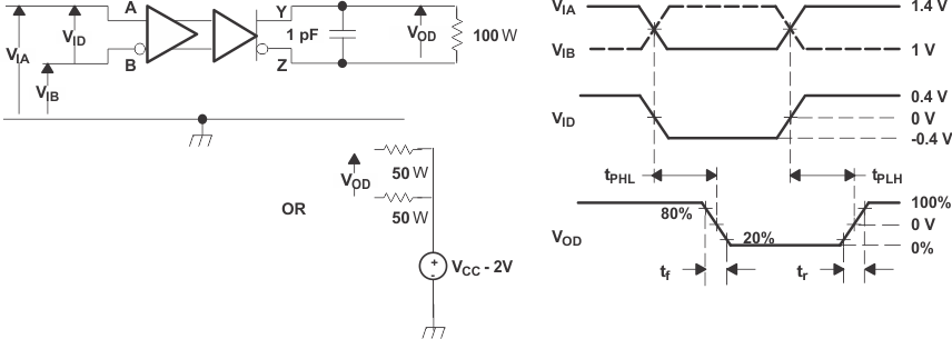
 Figure 31. SN65LVDx100 Differential Output Voltage (VOD) Test Circuit

NOTE:
All input pulses are supplied by a generator having the following characteristics: tr or tf ≤ 0.25 ns, pulse repetition rate (PRR) = 0.5 Mpps, pulse width = 500 ± 10 ns. CL includes instrumentation and fixture capacitance within 0.06 mm of the device under test. The measurement of VOC(PP) is made on test equipment with a –3 dB bandwidth of at least 300 MHz.
NOTE:
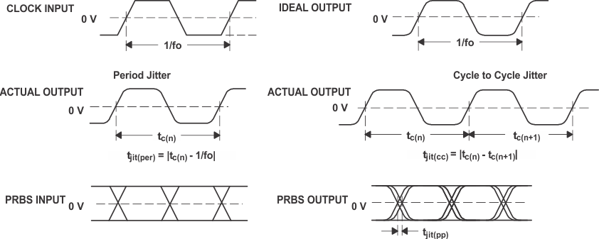
All input pulses are supplied by a generator having the following characteristics: tr or tf ≤ 0.25 ns, pulse repetition rate (PRR) = 50 Mpps, pulse width = 10 ± 0.2 ns. CL includes instrumentation and fixture capacitance within 0.06 mm of the device under test. Measurement equipment provides a bandwidth of 5 GHz minimum. Figure 34. Driver Jitter Measurement Waveforms

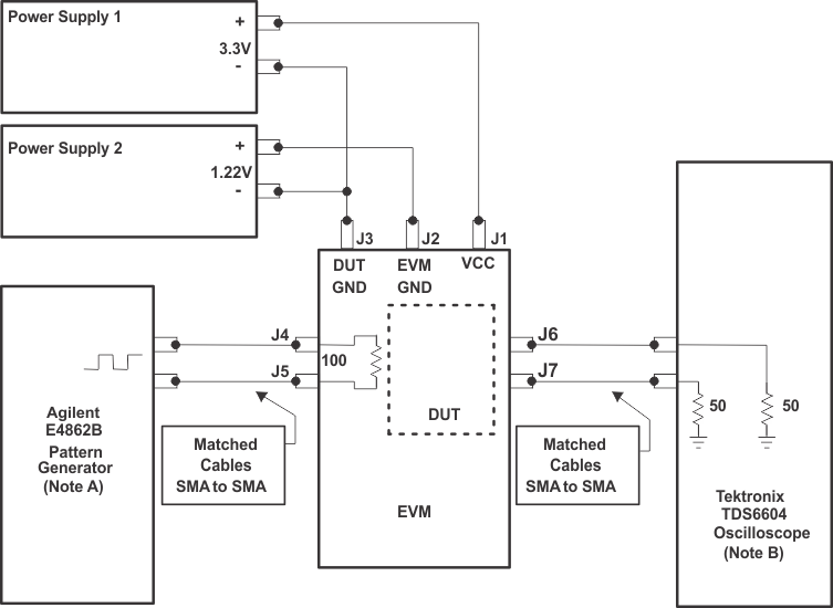
A. Source jitter is subtracted from the measured values.
B. TDS JIT3 jitter analysis software installed
Figure 35. Jitter Setup Connections for SN65LVDS100 and SN65LVDS101