SLLS261N July   1997  – April 2021 SN55LVDS31 , SN65LVDS31 , SN65LVDS3487 , SN65LVDS9638

PRODUCTION DATA  

  1. Features
  2. Applications
  3. Description
  4. Revision History
  5. Description (Continued)
  6. Pin Configuration and Functions
  7. Specifications
    1. 7.1 Absolute Maximum Ratings (1)
    2. 7.2 ESD Ratings
    3. 7.3 Recommended Operating Conditions
    4. 7.4 Thermal Information
    5. 7.5 Electrical Characteristics: SN55LVDS31
    6. 7.6 Electrical Characteristics: SN65LVDSxxxx
    7. 7.7 Switching Characteristics: SN55LVDS31
    8. 7.8 Switching Characteristics: SN65LVDSxxxx
    9. 7.9 Typical Characteristics
      1. 7.9.1 17
  8. Parameter Measurement Information
    1. 8.1 19
  9. Detailed Description
    1. 9.1 Overview
    2. 9.2 Functional Block Diagram
    3. 9.3 Feature Description
      1. 9.3.1 Driver Disabled Output
      2. 9.3.2 NC Pins
      3. 9.3.3 Unused Enable Pins
      4. 9.3.4 Driver Equivalent Schematics
    4. 9.4 Device Functional Modes
  10. 10Application and Implementation
    1. 10.1 Application Information
    2. 10.2 Typical Application
      1. 10.2.1 Point-to-Point Communications
        1. 10.2.1.1 Design Requirements
        2. 10.2.1.2 Detailed Design Procedure
          1. 10.2.1.2.1 Driver Supply Voltage
          2. 10.2.1.2.2 Driver Bypass Capacitance
          3. 10.2.1.2.3 Driver Output Voltage
          4. 10.2.1.2.4 Interconnecting Media
          5. 10.2.1.2.5 PCB Transmission Lines
          6. 10.2.1.2.6 Termination Resistor
          7. 10.2.1.2.7 Driver NC Pins
        3. 10.2.1.3 Application Curve
      2. 10.2.2 Multidrop Communications
        1. 10.2.2.1 Design Requirements
        2. 10.2.2.2 Detailed Design Procedure
          1. 10.2.2.2.1 Interconnecting Media
        3. 10.2.2.3 Application Curve
  11. 11Power Supply Recommendations
    1. 11.1 49
  12. 12Layout
    1. 12.1 Layout Guidelines
      1. 12.1.1 Microstrip vs. Stripline Topologies
      2. 12.1.2 Dielectric Type and Board Construction
      3. 12.1.3 Recommended Stack Layout
      4. 12.1.4 Separation Between Traces
      5. 12.1.5 Crosstalk and Ground Bounce Minimization
    2. 12.2 Layout Example
  13. 13Device and Documentation Support
    1. 13.1 Device Support
      1. 13.1.1 Other LVDS Products
    2. 13.2 Documentation Support
      1. 13.2.1 Related Information
      2. 13.2.2 Receiving Notification of Documentation Updates
      3. 13.2.3 Related Links
    3. 13.3 Support Resources
    4. 13.4 Trademarks
    5. 13.5 Electrostatic Discharge Caution
    6. 13.6 Glossary
  14. 14Mechanical, Packaging, and Orderable Information

Package Options

Refer to the PDF data sheet for device specific package drawings

Mechanical Data (Package|Pins)
  • D|16
Thermal pad, mechanical data (Package|Pins)
Orderable Information

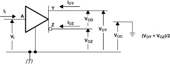
GUID-B826CF4E-AA36-4DB1-BD07-6CC6C3325F5E-low.gifFigure 8-1 Voltage and Current Definitions
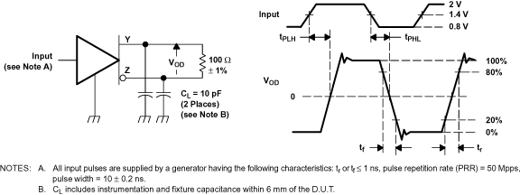
GUID-22C0BE66-7231-4F86-BB1A-F7BEFF351DE8-low.gifFigure 8-2 Test Circuit, Timing, and Voltage Definitions for the Differential Output Signal
GUID-207F0D87-4DAD-4AA2-86E7-23052D8D881C-low.gifFigure 8-3 Test Circuit and Definitions for the Driver Common-Mode Output Voltage
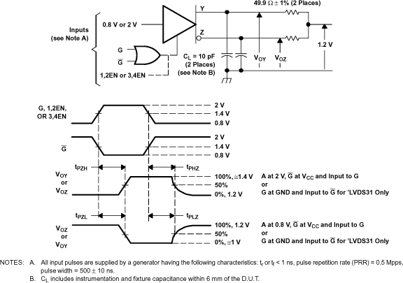
GUID-F57BE6B1-2E9E-4505-8469-143344274261-low.gifFigure 8-4 Enable or Disable Time Circuit and Definitions