SLLSF42A March   2018  – May 2018 SN65LVDS93B-Q1

PRODUCTION DATA.  

  1. Features
  2. Applications
  3. Description
    1.     Simplified Schematic
  4. Revision History
  5. Pin Configuration and Functions
    1.     Pin Functions
  6. Specifications
    1. 6.1 Absolute Maximum Ratings
    2. 6.2 ESD Ratings
    3. 6.3 Recommended Operating Conditions
    4. 6.4 Thermal Information
    5. 6.5 Electrical Characteristics
    6. 6.6 Timing Requirements
    7. 6.7 Switching Characteristics
    8. 6.8 Typical Characteristics
  7. Parameter Measurement Information
  8. Detailed Description
    1. 8.1 Overview
    2. 8.2 Functional Block Diagram
    3. 8.3 Feature Description
      1. 8.3.1 TTL Input Data
      2. 8.3.2 LVDS Output Data
    4. 8.4 Device Functional Modes
      1. 8.4.1 Input Clock Edge
      2. 8.4.2 Low Power Mode
  9. Application and Implementation
    1. 9.1 Application Information
    2. 9.2 Typical Application
      1. 9.2.1 Design Requirements
      2. 9.2.2 Detailed Design Procedure
        1. 9.2.2.1 Power Up Sequence
        2. 9.2.2.2 Signal Connectivity
        3. 9.2.2.3 PCB Routing
      3. 9.2.3 Application Curve
  10. 10Power Supply Recommendations
  11. 11Layout
    1. 11.1 Layout Guidelines
      1. 11.1.1 Board Stackup
      2. 11.1.2 Power and Ground Planes
      3. 11.1.3 Traces, Vias, and Other PCB Components
    2. 11.2 Layout Example
  12. 12Device and Documentation Support
    1. 12.1 Trademarks
    2. 12.2 Electrostatic Discharge Caution
    3. 12.3 Receiving Notification of Documentation Updates
    4. 12.4 Community Resources
    5. 12.5 Glossary
  13. 13Mechanical, Packaging, and Orderable Information

Package Options

Mechanical Data (Package|Pins)
Thermal pad, mechanical data (Package|Pins)
Orderable Information

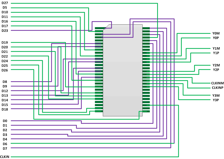
PCB Routing

Figure 16 shows a possible breakout of the data input and output signals on two layers of a printed circuit board.

SN65LVDS93B-Q1 PCB_routing_sllsem1.gifFigure 16. Printed Circuit Board Routing Example (See Figure 12 for the Schematic)