SLLS373M July 1999 – March 2024 SN65LVDS1 , SN65LVDS2 , SN65LVDT2
PRODUCTION DATA
- 1
- 1 Features
- 2 Applications
- 3 Description
- 4 Device Options
- 5 Pin Configuration and Functions
- 6 Specifications
- 7 Parameter Measurement Information
- 8 Detailed Description
-
9 Application and Implementation
- 9.1 Application Information
- 9.2
Typical Applications
- 9.2.1
Point-to-Point Communications
- 9.2.1.1 Design Requirements
- 9.2.1.2
Detailed Design Procedure
- 9.2.1.2.1 Driver Supply Voltage
- 9.2.1.2.2 Driver Bypass Capacitance
- 9.2.1.2.3 Driver Input Voltage
- 9.2.1.2.4 Driver Output Voltage
- 9.2.1.2.5 Interconnecting Media
- 9.2.1.2.6 PCB Transmission Lines
- 9.2.1.2.7 Termination Resistor
- 9.2.1.2.8 Driver NC Pins
- 9.2.1.2.9 Receiver Supply Voltage
- 9.2.1.2.10 Receiver Bypass Capacitance
- 9.2.1.2.11 Receiver Input Common-Mode Range
- 9.2.1.2.12 Receiver Input Signal
- 9.2.1.2.13 Receiver Output Signal
- 9.2.1.2.14 Receiver NC Pins
- 9.2.2 Application Curve
- 9.2.3 Multidrop Communications
- 9.2.1
Point-to-Point Communications
- 10Power Supply Recommendations
- 11Layout
- 12Device and Documentation Support
- 13Revision History
- 14Mechanical, Packaging, and Orderable Information
Package Options
Refer to the PDF data sheet for device specific package drawings
Mechanical Data (Package|Pins)
- D|8
- DBV|5
Thermal pad, mechanical data (Package|Pins)
Orderable Information
8.3.1.5 Driver Equivalent Schematics
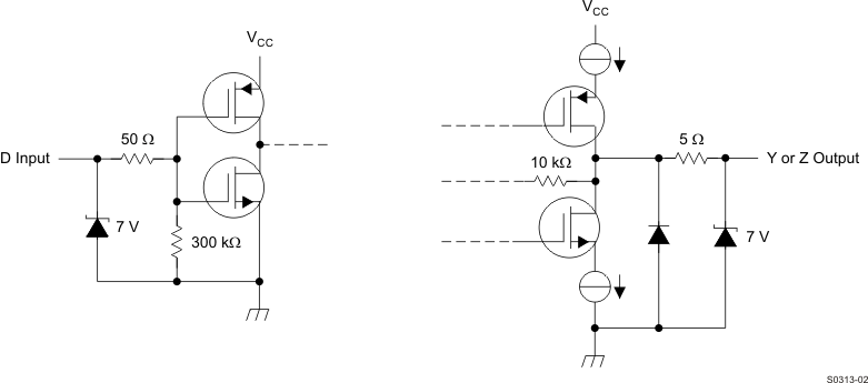
The SN65LVDS1 equivalent input and output schematic diagrams are shown in Figure 8-1. The driver input is represented by a CMOS inverter stage with a 7-V Zener diode. The input stage is high-impedance, and includes an internal pulldown to ground. If the driver input is left open, the driver input provides a low-level signal to the rest of the driver circuitry, resulting in a low-level signal at the driver output pins. The Zener diode provides ESD protection. The driver output stage is a differential pair, one half of which is shown in Figure 8-1. Like the input stage, the driver output includes a Zener diode for ESD protection. The schematic shows an output stage that includes a set of current sources (nominally 3.5 mA) that are connected to the output load circuit based upon the input stage signal. To the first order, the SN65LVDS2 output stage acts a constant-current source.
 Figure 8-1 Driver
Equivalent Input and Output Schematic Diagrams