SLLS902A February 2010 – March 2024 SN65MLVD040
PRODUCTION DATA
- 1
- 1 Features
- 2 Applications
- 3 Description
- 4 Pin Configuration and Functions
-
5 Specifications
- 5.1 Absolute Maximum Ratings
- 5.2 Reccommended Operationg Conditions
- 5.3 Thermal Characteristics
- 5.4 Package Dissipation Ratings
- 5.5 Device Electrical Characteristics
- 5.6 Driver Electrical Characteristics
- 5.7 Reciver Electrical Charecteristics
- 5.8 Bus Input and Output Electrical Characteristics
- 5.9 Driver Switching Characterisitics
- 5.10 Reciever Switching Charecteristics
- 5.11 Typical Characteristics
- 6 Paramater Measurement Information
- 7 Application and Implementation
- 8 Device and Documentation Support
- 9 Revision History
- 10Mechanical, Packaging, and Orderable Information
Package Options
Mechanical Data (Package|Pins)
- RGZ|48
Thermal pad, mechanical data (Package|Pins)
- RGZ|48
Orderable Information
6 Paramater Measurement Information
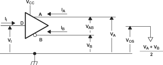 Figure 6-1 Driver
Voltage and Current Definitions
All resistors
are 1% tolerance.
Figure 6-2 Differential Output Voltage Test Circuit
A. All input pulses are supplied by a
generator having the following characteristics: tr or tf ≤
1 ns, pulse frequency = 1 MHz, duty cycle = 50 ±5%.
B. C1, C2 and C3 include
instrumentation and fixture capacitance within 2 cm of the D.U.T. and are
±20%.
C. R1 and R2 are metal film, surface
mount, ±1%, and located within 2 cm of the D.U.T.
D. The measurement of
VOS(PP) is made on test equipment with a –3 dB bandwidth of at
least 1 GHz.
Figure 6-3 Test
Circuit and Definitions for the Driver Common-Mode Output Voltage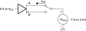 Figure 6-4 Driver
Short-Circuit Test Circuit
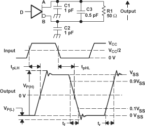
A. All input pulses are supplied by a
generator having the following characteristics: tr or tf ≤
1 ns, frequency = 1 MHz, duty cycle = 50 ±5%.
B. C1, C2, and C3 include
instrumentation and fixture capacitance within 2 cm of the D.U.T. and are
±20%.
C. R1 is a metal film, surface mount,
and 1% tolerance and located within 2 cm of the D.U.T.
D. The measurement is made on test
equipment with a –3 dB bandwidth of at least 1 GHz.
Figure 6-5 Driver
Test Circuit, Timing, and Voltage Definitions for the Differential Output
Signal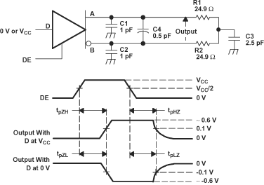
A. All input pulses are supplied by a
generator having the following characteristics: tr or tf ≤
1 ns, frequency = 1 MHz, duty cycle = 50 ±5%.
B. C1, C2, C3, and C4 includes
instrumentation and fixture capacitance within 2 cm of the D.U.T. and are
±20%.
C. R1 and R2 are metal film, surface
mount, and 1% tolerance and located within 2 cm of the D.U.T.
D. The measurement is made on test
equipment with a –3 dB bandwidth of at least 1 GHz.
Figure 6-6 Driver
Enable and Disable Time Circuit and Definitions Figure 6-7 Maximum
Steady State Output Voltage
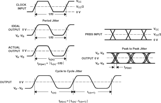
A. All input pulses are supplied by the
Agilent 81250 Parallel BERT Stimulus System with plug-in E4832A.
B. The cycle-to-cycle measurement is
made on a TEK TDS6604 running TDSJIT3 application software.
C. All other jitter measurements are
made with an Agilent Infiniium DCA-J 86100C Digital Communications Analyzer.
D. Period jitter and cycle-to-cycle
jitter are measured using a 125 MHz 50 ±1% duty cycle clock input. Measured over
75K samples.
E. Deterministic jitter and random
jitter are measured using a 250 Mbps 215–1 PRBS input. Measured over
BER = 10-12
Figure 6-8 Driver
Jitter Measurement Waveforms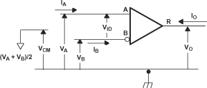 Figure 6-9 Receiver
Voltage and Current Definitions
Figure 6-9 Receiver
Voltage and Current DefinitionsTable 6-1 Type-1 Receiver Input
Threshold Test Voltages
| APPLIED VOLTAGES | RESULTING DIFFERENTIAL INPUT VOLTAGE |
RESULTING COMMON- MODE INPUT VOLTAGE |
RECEIVER OUTPUT(1) |
|
|---|---|---|---|---|
| VIA | VIB | VID | VIC | |
| 2.400 | 0.000 | 2.400 | 1.200 | H |
| 0.000 | 2.400 | –2.400 | 1.200 | L |
| 3.400 | 3.365 | 0.035 | 3.3825 | H |
| 3.365 | 3.400 | –0.035 | 3.3825 | L |
| –0.965 | –1 | 0.035 | –0.9825 | H |
| –1 | –0.965 | –0.035 | –0.9825 | L |
(1) H= high level, L = low level, output state assumes receiver is
enabled ( RE = L)
Table 6-2 Type-2 Receiver Input
Threshold Test Voltages
| APPLIED VOLTAGES | RESULTING DIFFERENTIAL INPUT VOLTAGE |
RESULTING COMMON- MODE INPUT VOLTAGE |
RECEIVER OUTPUT(1) |
|
|---|---|---|---|---|
| VIA | VIB | VID | VIC | |
| 2.400 | 0.000 | 2.400 | 1.200 | H |
| 0.000 | 2.400 | –2.400 | 1.200 | L |
| 3.400 | 3.265 | 0.135 | 3.3325 | H |
| 3.4000 | 3.335 | 0.065 | 3.3675 | L |
| –0.865 | –1 | 0.135 | –0.9325 | H |
| –0.935 | –1 | 0.065 | –0.9675 | L |
(1) H= high level, L = low level, output state assumes receiver is
enabled ( RE = L)
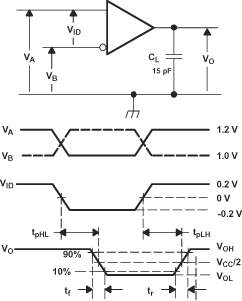
A. All input pulses are supplied by a
generator having the following characteristics: tr or tf ≤
1 ns, frequency = 1 MHz, duty cycle = 50 ±5%. CL is a combination of
a 20%-tolerance, low-loss ceramic, surface-mount capacitor and fixture
capacitance within 2 cm of the D.U.T.
B. The measurement is made on test
equipment with a –3 dB bandwidth of at least 1 GHz.
Figure 6-10 Receiver
Timing Test Circuit and Waveforms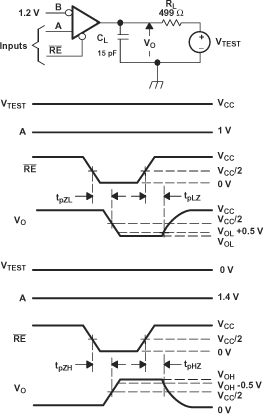
A. All input pulses are supplied by a
generator having the following characteristics: tr or tf≤
1 ns, frequency = 1 MHz, duty cycle = 50 ± 5%.
B. RL is 1% tolerance, metal
film, surface mount, and located within 2 cm of the D.U.T.
C. CL is the instrumentation
and fixture capacitance within 2 cm of the DUT and ±20%. The measurement is made
on test equipment with a –3 dB bandwidth of at least 1 GHz.
Figure 6-11 Receiver
Enable/Disable Time Test Circuit and Waveforms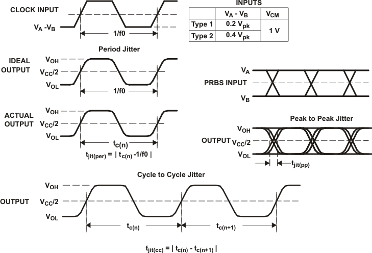
A. All input pulses are supplied by
the Agilent 81250 Parallel BERT Stimulus System with plug-in E4832A.
B. The cycle-to-cycle measurement is
made on a TEK TDS6604 running TDSJIT3 application software.
C. All other jitter measurements are
made with an Agilent Infiniium DCA-J 86100C Digital Communications
Analyzer.
D. Period jitter and cycle-to-cycle
jitter are measured using a 125 MHz 50 ±1% duty cycle clock input. Measured over
75K samples.
E. Deterministic jitter and random
jitter are measured using a 250 Mbps 215–1 PRBS input. Measured over
BER = 10-12
Figure 6-12 Receiver
Jitter Measurement Waveforms