SLLS902A February 2010 – March 2024 SN65MLVD040
PRODUCTION DATA
- 1
- 1 Features
- 2 Applications
- 3 Description
- 4 Pin Configuration and Functions
-
5 Specifications
- 5.1 Absolute Maximum Ratings
- 5.2 Reccommended Operationg Conditions
- 5.3 Thermal Characteristics
- 5.4 Package Dissipation Ratings
- 5.5 Device Electrical Characteristics
- 5.6 Driver Electrical Characteristics
- 5.7 Reciver Electrical Charecteristics
- 5.8 Bus Input and Output Electrical Characteristics
- 5.9 Driver Switching Characterisitics
- 5.10 Reciever Switching Charecteristics
- 5.11 Typical Characteristics
- 6 Paramater Measurement Information
- 7 Application and Implementation
- 8 Device and Documentation Support
- 9 Revision History
- 10Mechanical, Packaging, and Orderable Information
Package Options
Mechanical Data (Package|Pins)
- RGZ|48
Thermal pad, mechanical data (Package|Pins)
- RGZ|48
Orderable Information
7.1.1.1 Live Insertion/Glitch-Free Power Up/Down
The SN65MLVD040 family of products offered by Texas Instruments provides a glitch-free powerup/down feature that prevents the M-LVDS outputs of the device from turning on during a powerup or powerdown event. This is especially important in live insertion applications, when a device is physically connected to an M-LVDS multipoint bus and VCC is ramping.
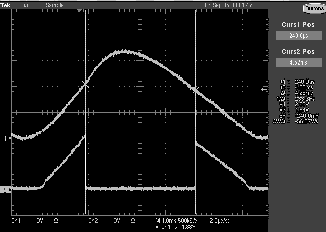
While the M-LVDS interface for these devices is glitch free on powerup/down, the receiver output structure is not. Figure 7-2 shows the performance of the receiver output pin, R (CHANNEL 2), as VCC (CHANNEL 1) is ramped.
 Figure 7-2 M-LVDS Receiver Output: VCC (CHANNEL 1), R Pin (CHANNEL 2)
The glitch on the R pin is independent of the RE voltage. Any complications or issues from this glitch are resolved in power sequencing or system requirements that suspend operation until VCC has reached a steady state value.