SLLS736B July 2006 – March 2024 SN65MLVD047A
PRODUCTION DATA
- 1
- 1 Features
- 2 Applications
- 3 Description
- 4 Pin Configuration
- 5 Specifications
- 6 Parameter Measurement Information
- 7 Device Functional Modes
- 8 Application and Implementation
- 9 Device and Documentation Support
- 10Revision History
- 11Mechanical, Packaging, and Orderable Information
Package Options
Mechanical Data (Package|Pins)
Thermal pad, mechanical data (Package|Pins)
Orderable Information
6 Parameter Measurement Information
 Figure 6-1 Driver Voltage and Current Definitions
All resistors are 1% tolerance.
Figure 6-2 Differential Output Voltage Test Circuit
A. All input pulses are supplied by a generator having
the following characteristics: tr or tf ≤ 1ns, pulse
frequency = 500kHz, duty cycle = 50 ± 5%.
B. C1, C2 and C3 include instrumentation and fixture capacitance within 2 cm of the D.U.T. and are ±20%.
C. R1 and R2 are metal film, surface mount, ±1%, and located within 2 cm of the D.U.T.
D. The measurement of VOS(PP) is made on
test equipment with a –3dB bandwidth of at least 1 GHz.
Figure 6-3 Test Circuit and Definitions for the Common-Mode Output Voltage Figure 6-4 Short-Circuit Test Circuit
A. All input pulses are supplied by a generator having
the following characteristics: tr or tf ≤ 1ns, frequency =
500kHz, duty cycle = 50 ± 5%.
B. C1, C2, and C3 include instrumentation and fixture capacitance within 2 cm of the D.U.T. and are ±20%.
C. R1 is a metal film, surface mount, and 1% tolerance and located within 2 cm of the D.U.T.
D. The measurement is made on test equipment with a
–3dB bandwidth of at least 1 GHz.
Figure 6-5 Driver Test Circuit, Timing, and Voltage Definitions for the Differential Output Signal
A. All input pulses are supplied by a generator having
the following characteristics: tr or tf ≤ 1ns, frequency =
500kHz, duty cycle = 50 ± 5%.
B. C1, C2, C3, and C4 includes instrumentation and fixture capacitance within 2 cm of the D.U.T. and are ±20%.
C. R1 and R2 are metal film, surface mount, and 1% tolerance and located within 2 cm of the D.U.T.
D. The measurement is made on test equipment with a
–3dB bandwidth of at least 1GHz.
Figure 6-6 Driver Enable and Disable Time Circuit and Definitions Figure 6-7 Driver Maximum Steady State Output Voltage
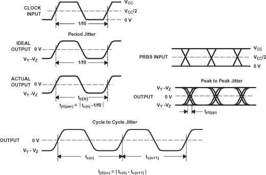
A. All input pulses are supplied by an Agilent 8304A Stimulus System.
B. The measurement is made on a TEK TDS6604 running TDSJIT3 application software
C. Period jitter and cycle-to-cycle jitter are measured
using a 100MHz 50 ±1% duty cycle clock input.
D. Peak-to-peak jitter is measured using a 200Mbps
215 – 1PRBS input.
Figure 6-8 Driver Jitter Measurement Waveforms