SLLS573E December 2003 – March 2024 SN65MLVD200A , SN65MLVD202A , SN65MLVD204A , SN65MLVD205A
PRODUCTION DATA
- 1
- 1 Features
- 2 Applications
- 3 Description
- 4 Device Comparison Table
- 5 Pin Configuration and Functions
-
6 Specifications
- 6.1 Absolute Maximum Ratings
- 6.2 ESD Ratings
- 6.3 Recommended Operating Conditions
- 6.4 Thermal Information
- 6.5 Electrical Characteristics
- 6.6 Electrical Characteristics – Driver
- 6.7 Electrical Characteristics – Receiver
- 6.8 Electrical Characteristics – BUS Input and Output
- 6.9 Switching Characteristics – Driver
- 6.10 Switching Characteristics – Receiver
- 6.11 Typical Characteristics
- 7 Parameter Measurement Information
- 8 Detailed Description
-
9 Application and Implementation
- 9.1 Application Information
- 9.2
Typical Application
- 9.2.1 Design Requirements
- 9.2.2
Detailed Design Procedure
- 9.2.2.1 Supply Voltage
- 9.2.2.2 Supply Bypass Capacitance
- 9.2.2.3 Driver Input Voltage
- 9.2.2.4 Driver Output Voltage
- 9.2.2.5 Termination Resistors
- 9.2.2.6 Receiver Input Signal
- 9.2.2.7 Receiver Input Threshold (Failsafe)
- 9.2.2.8 Receiver Output Signal
- 9.2.2.9 Interconnecting Media
- 9.2.2.10 PCB Transmission Lines
- 9.2.3 Application Curves
- 10Power Supply Recommendations
- 11Layout
- 12Device and Documentation Support
- 13Revision History
- 14Mechanical, Packaging, and Orderable Information
Package Options
Refer to the PDF data sheet for device specific package drawings
Mechanical Data (Package|Pins)
- D|14
Thermal pad, mechanical data (Package|Pins)
Orderable Information
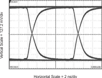
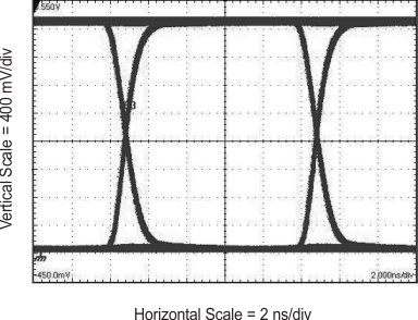
9.2.3 Application Curves

| 100 Mbps | 215 –1 PRBS | RL = 50 Ω |

| 100 Mbps | 215 –1 PRBS | CL = 15 pF |