SCASE13 July 2024 SN74AC16
PRODUCTION DATA
- 1
- 1 Features
- 2 Applications
- 3 Description
- 4 Pin Configuration and Functions
- 5 Specifications
- 6 Parameter Measurement Information
- 7 Detailed Description
- 8 Application and Implementation
- 9 Device and Documentation Support
- 10Revision History
- 11Mechanical, Packaging, and Orderable Information
Package Options
Mechanical Data (Package|Pins)
Thermal pad, mechanical data (Package|Pins)
- BQA|14
Orderable Information
4 Pin Configuration and Functions
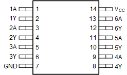
 Figure 4-1 SN74AC16 PW
Package, 14-Pin TSSOP (Top View)
 Figure 4-2 BQA Package, 14-Pin WQFN (Top
View)
Figure 4-2 BQA Package, 14-Pin WQFN (Top
View)Table 4-1 Pin Functions
| PIN | TYPE(1) | DESCRIPTION | |
|---|---|---|---|
| NAME | NO. | ||
| 1A | 1 | I | Channel 1 input |
| 1Y | 2 | O | Channel 1 output |
| 2A | 3 | I | Channel 2 input |
| 2Y | 4 | O | Channel 2 output |
| 3A | 5 | I | Channel 3 input |
| 3Y | 6 | O | Channel 3 output |
| GND | 7 | G | Ground |
| 4Y | 8 | O | Channel 4 output |
| 4A | 9 | I | Channel 4 input |
| 5Y | 10 | O | Channel 5 output |
| 5A | 11 | I | Channel 5 input |
| 6Y | 12 | O | Channel 6 output |
| 6A | 13 | I | Channel 6 input |
| VCC | 14 | P | Positive supply |
| Thermal pad(2) | — | The thermal pad can be connected to GND or left floating. Do not connect to any other signal or supply | |
(1) Signal Types: I = Input, O = Output, I/O
= Input or Output, P = Power, G = Ground
(2) BQA Package only.