SCAS956D May 2023 – March 2024 SN74AC244-Q1
PRODUCTION DATA
- 1
- 1 Features
- 2 Applications
- 3 Description
- 4 Pin Configuration and Functions
-
5 Specifications
- 5.1 Absolute Maximum Ratings
- 5.2 ESD Ratings
- 5.3 Recommended Operating Conditions
- 5.4 Thermal Information
- 5.5 Electrical Characteristics
- 5.6 Switching Characteristics 1.5-V VCC
- 5.7 Switching Characteristics 1.8-V VCC
- 5.8 Switching Characteristics 2.5-V VCC
- 5.9 Switching Characteristics 3.3-V VCC
- 5.10 Switching Characteristics 5-V VCC
- 5.11 Noise Characteristics
- 5.12 Typical Characteristics
- 6 Parameter Measurement Information
- 7 Detailed Description
- 8 Application Information Disclaimer
- 9 Device and Documentation Support
- 10Revision History
- 11Mechanical, Packaging, and Orderable Information
Package Options
Refer to the PDF data sheet for device specific package drawings
Mechanical Data (Package|Pins)
- RKS|20
- DGS|20
- PW|20
Thermal pad, mechanical data (Package|Pins)
- RKS|20
Orderable Information
3 Description
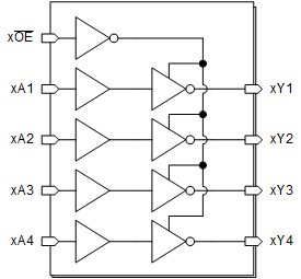
The SN74AC244-Q1 is an octal buffer with 3-state outputs and Schmitt-trigger inputs. The device is configured into two banks of four drivers, each controlled by an output enable pin.
Package Information
| PART NUMBER | PACKAGE(1) | PACKAGE SIZE(2) | BODY SIZE(3) |
|---|---|---|---|
| SN74AC244-Q1 | DGS (VSSOP, 20) | 5.1mm × 4.9mm | 5.1mm × 3mm |
| RKS (VQFN, 20) | 4.5mm × 2.5mm | 4.5mm × 2.5mm | |
| PW (TSSOP, 20) | 6.5mm × 6.4mm | 6.5mm × 4.4mm |
(1) For more information, see Section 11.
(2) The package size (length × width) is a nominal value and includes pins, where
applicable.
(3) The body size (length × width) is a nominal value and does not include pins.
 Logic Diagram (Positive Logic)