SCLS971B August 2023 – March 2024 SN74AC245-Q1
PRODUCTION DATA
- 1
- 1 Features
- 2 Applications
- 3 Description
- 4 Pin Configuration and Functions
- 5 Specifications
- 6 Parameter Measurement Information
- 7 Detailed Description
- 8 Application Information Disclaimer
- 9 Device and Documentation Support
- 10Revision History
- 11Mechanical, Packaging, and Orderable Information
Package Options
Refer to the PDF data sheet for device specific package drawings
Mechanical Data (Package|Pins)
- RKS|20
- DGS|20
- PW|20
Thermal pad, mechanical data (Package|Pins)
- RKS|20
Orderable Information
3 Description
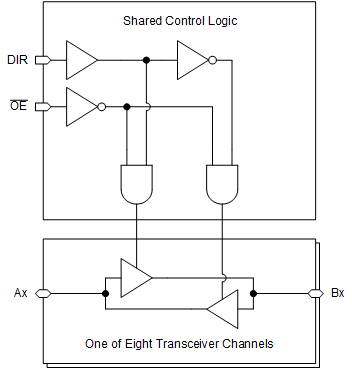
The SN74AC245-Q1 is an octal bus transceiver with 3-state outputs. All eight channels are controlled by the direction (DIR) pin and output enable (OE) pin.
Package Information
| PART NUMBER | PACKAGE(1) | PACKAGE SIZE(2) | BODY SIZE(3) |
|---|---|---|---|
| SN74AC245-Q1 | DGS (VSSOP, 20) | 5.1mm × 4.9mm | 5.1mm × 3mm |
| PW (TSSOP, 20) | 6.5mm × 6.4mm | 6.5mm × 4.4mm | |
| RKS (VQFN, 20) | 4.5mm × 2.5mm | 4.5mm × 2.5mm |
(1) For all available packages, see the orderable addendum at the end of the data sheet.
(2) The package size (length × width) is a nominal value and includes pins, where applicable
(3) The body size (length × width) is a nominal value and does not include pins.
 Logic Diagram (Positive Logic)