SCAS461I February 1995 – April 2024 SN54AC245 , SN74AC245
PRODMIX
- 1
- 1 Features
- 2 Applications
- 3 Description
- 4 Pin Configuration and Functions
- 5 Specifications
- 6 Parameter Measurement Information
- 7 Detailed Description
- 8 Application Information Disclaimer
- 9 Device and Documentation Support
- 10Revision History
- 11Mechanical, Packaging, and Orderable Information
Package Options
Refer to the PDF data sheet for device specific package drawings
Mechanical Data (Package|Pins)
- DB|20
- RKS|20
- NS|20
- N|20
- DGS|20
- DW|20
- PW|20
Thermal pad, mechanical data (Package|Pins)
- RKS|20
Orderable Information
3 Description
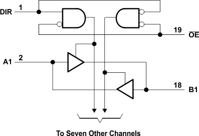
The 'AC245 octal bus transceivers are designed for asynchronous two-way communication between data buses. The control-function implementation minimizes external timing requirements.
The devices allow data transmission from the A bus to the B bus or from the B bus to the A bus, depending on the logic level at the direction-control (DIR) input. The output-enable (OE) input can be used to disable the device so that the buses are effectively isolated.
Device Information
| PART NUMBER | PACKAGE(1) | PACKAGE SIZE(2) | BODY SIZE(3) |
|---|---|---|---|
| SNx4AC245 | DB (SSOP, 20) | 7.2mm × 7.8mm | 7.2mm × 5.3mm |
| DGS (VSSOP, 20) | 5.1mm × 4.9mm | 5.1mm × 3mm | |
| DW (SOIC, 20) | 12.8mm × 10.3mm | 12.8mm × 7.5mm | |
| N (PDIP, 20) | 24.33mm × 9.4mm | 24.33mm × 6.35mm | |
| NS (SO, 20) | 12.6mm × 7.8mm | 12.6mm × 5.3mm | |
| PW (TSSOP, 20) | 6.5mm × 6.4mm | 6.5mm × 4.4mm | |
| RKS (VQFN, 20) | 4.5mm × 2.5mm | 4.5mm × 2.5mm |
(1) For more information, see Section 11.
(2) The package size (length ×
width) is a nominal value and includes pins, where applicable.
(3) The body size (length × width) is
a nominal value and does not include pins.
 Logic Diagram (Positive
Logic)