SCASE16 September 2024 SN74AC2G100
ADVANCE INFORMATION
- 1
- 1 Features
- 2 Applications
- 3 Description
- 4 Pin Configuration and Functions
- 5 Specifications
- 6 Parameter Measurement Information
- 7 Detailed Description
- 8 Application and Implementation
- 9 Device and Documentation Support
- 10Revision History
- 11Mechanical, Packaging, and Orderable Information
Package Options
Mechanical Data (Package|Pins)
- BQB|16
Thermal pad, mechanical data (Package|Pins)
Orderable Information
5.8 Typical Characteristics
TA = 25°C (unless otherwise noted)
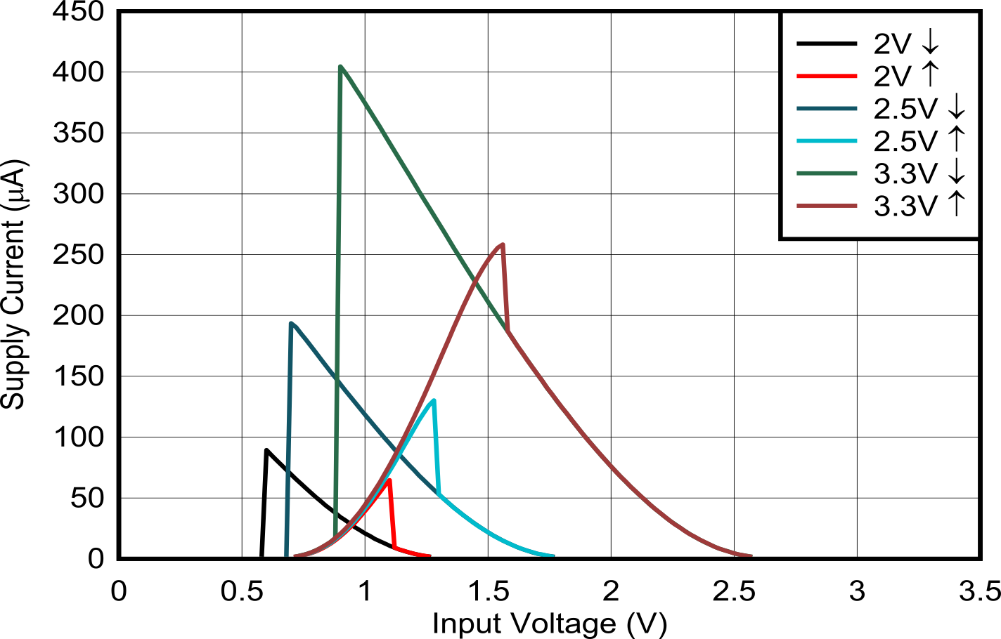
 Figure 5-1 Supply Current Across Input Voltage 1.8V and 2.5V Supply
 Figure 5-3 Supply Current Across Supply Voltage
 Figure 5-5 Output Voltage vs Current in LOW State
 Figure 5-7 Output Voltage vs Current in LOW State; 5V Supply
 Figure 5-9 Output Voltage vs Current in LOW State; 3.3V Supply
 Figure 5-11 Output Voltage vs Current in LOW State; 2.5V Supply
 Figure 5-13 Output Voltage vs Current in LOW State; 1.8V Supply
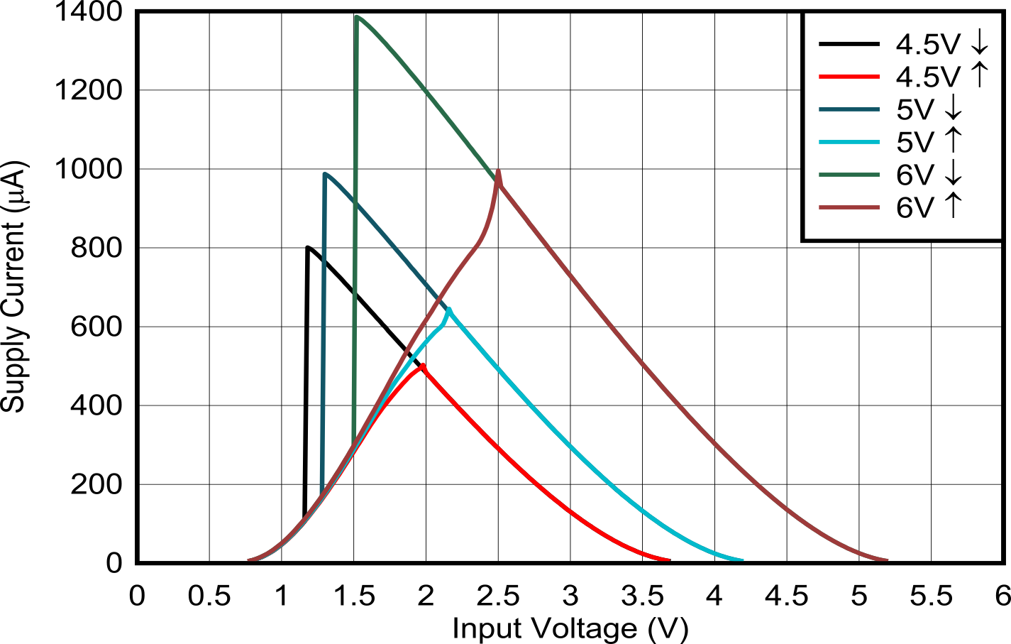
 Figure 5-2 Supply Current Across Input Voltage 3.3V and 5.0V Supply
 Figure 5-4 Output Voltage vs Current in HIGH State
 Figure 5-6 Output Voltage vs Current in HIGH State; 5V Supply
 Figure 5-8 Output Voltage vs Current in HIGH State; 3.3V Supply
 Figure 5-10 Output Voltage vs Current in HIGH State; 2.5V Supply
 Figure 5-12 Output Voltage vs Current in HIGH State; 1.8V Supply