SCLSA24 June 2024 SN74AC595
PRODUCTION DATA
- 1
- 1 Features
- 2 Applications
- 3 Description
- 4 Pin Configuration and Functions
- 5 Specifications
- 15
- 6 Parameter Measurement Information
- 7 Detailed Description
- 8 Application and Implementation
- 9 Device and Documentation Support
- 10Revision History
- 11Mechanical, Packaging, and Orderable Information
Package Options
Refer to the PDF data sheet for device specific package drawings
Mechanical Data (Package|Pins)
- BQB|16
- PW|16
Thermal pad, mechanical data (Package|Pins)
- BQB|16
Orderable Information
6 Parameter Measurement Information
Phase relationships between waveforms were chosen arbitrarily for the examples listed in the following table. All input pulses are supplied by generators having the following characteristics: PRR ≤ 1MHz, ZO = 50Ω, tt < 2.5ns.
For clock inputs, fmax is measured when the input duty cycle is 50%.
The outputs are measured individually with one input transition per measurement.
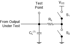
| TEST | S1 | S2 | RL | CL | ΔV | VCC |
|---|---|---|---|---|---|---|
| tPLH, tPHL | OPEN | OPEN | — | 2.5ns | — | ALL |
| tPLZ, tPZL | CLOSED | OPEN | 500Ω | 2.5ns | 0.15V | ≤ 2.5V |
| tPHZ, tPZH | OPEN | CLOSED | 500Ω | 2.5ns | 0.15V | ≤ 2.5V |
| tPLZ, tPZL | CLOSED | OPEN | 500Ω | 2.5ns | 0.3V | > 2.5V |
| tPHZ, tPZH | OPEN | CLOSED | 500Ω | 2.5ns | 0.3V | > 2.5V |

(1) CL includes probe
and test-fixture capacitance.
Figure 6-1 Load Circuit for 3-State
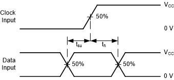
Outputs Figure 6-3 Voltage Waveforms, Setup
and Hold Times
(3) The greater between
tPZL and tPZH is the same as
ten.
(4) The greater between
tPLZ and tPHZ is the same as
tdis.
Figure 6-5 Voltage Waveforms
Propagation Delays Figure 6-2 Voltage Waveforms, Pulse
Duration
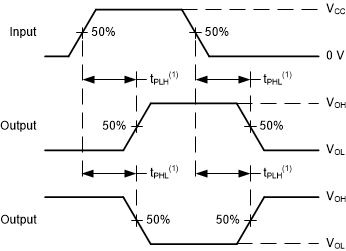
(1) The
greater between tPLH and tPHL is the same as
tpd.
Figure 6-4 Voltage Waveforms
Propagation Delays
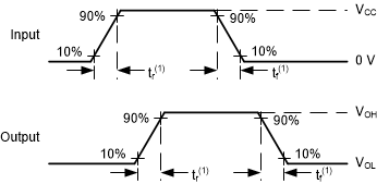
(1) The greater between
tr and tf is the same as tt.
Figure 6-6 Voltage Waveforms, Input
and Output Transition Times