SCASE09 June 2024 SN74ACT138-Q1
PRODUCTION DATA
- 1
- 1 Features
- 2 Applications
- 3 Description
- 4 Pin Configuration and Functions
- 5 Specifications
- 6 Parameter Measurement Information
- 7 Detailed Description
- 8 Application and Implementation
- 9 Device and Documentation Support
- 10Revision History
- 11Mechanical, Packaging, and Orderable Information
Package Options
Refer to the PDF data sheet for device specific package drawings
Mechanical Data (Package|Pins)
- PW|16
- BQB|16
Thermal pad, mechanical data (Package|Pins)
- BQB|16
Orderable Information
3 Description
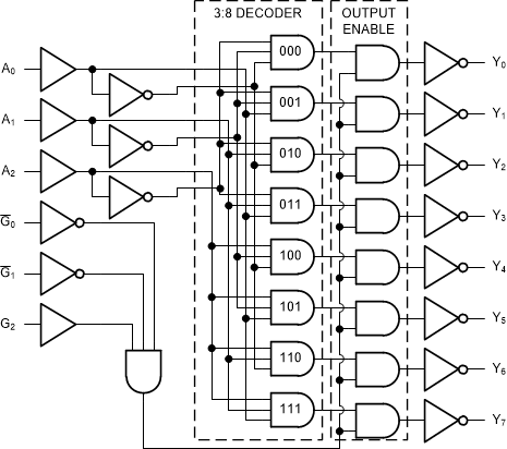
The SN74ACT138-Q1 contains a three to eight decoder with one standard output strobe (G2) and two active low output strobes (G1 and G0). When the outputs are gated by any of the strobe inputs, they are all forced into the high state. When the outputs are not disabled by the strobe inputs, only the selected output is low while all others are high. TTL-compatible CMOS inputs provide the capability to up-translate input signals from as low as 2V up to 5V outputs.
Package Information
| PART NUMBER | PACKAGE(1) | PACKAGE SIZE(2) | BODY SIZE(3) |
|---|---|---|---|
| SN74ACT138-Q1 | PW (TSSOP, 16) | 5mm × 6.4mm | 5mm × 4.4mm |
| BQB (WQFN, 16) | 3.5mm × 2.5mm | 3.5mm × 2.5mm |
(1) For more information, see Section 11.
(2) The package size (length x width) is a nominal value and includes
pins, where applicable.
(3) The body size (length × width) is a nominal value and does not
include pins.
 Logic Diagram (Positive Logic)