SCPS306 October   2024 SN74ACT174-Q1

PRODUCTION DATA  

  1.   1
  2. Features
  3. Applications
  4. Description
  5. Pin Configuration and Functions
  6. Specifications
    1. 5.1 Absolute Maximum Ratings
    2. 5.2 Electrical Characteristics
    3. 5.3 ESD Ratings
    4. 5.4 Recommended Operating Conditions
    5. 5.5 Switching Characteristics
    6. 5.6 Thermal Information
    7. 5.7 Timing Characteristics
    8. 5.8 Typical Characteristics
  7. Parameter Measurement Information
  8. Detailed Description
    1. 7.1 Overview
    2. 7.2 Functional Block Diagram
    3. 7.3 Feature Description
      1. 7.3.1 Balanced CMOS Push-Pull Outputs
      2. 7.3.2 Latching Logic
      3. 7.3.3 Wettable Flanks
      4. 7.3.4 Clamp Diode Structure
    4. 7.4 Device Functional Modes
  9. Application and Implementation
    1. 8.1 Application Information
    2. 8.2 Typical Application
      1. 8.2.1 Design Requirements
        1. 8.2.1.1 Power Considerations
        2. 8.2.1.2 Input Considerations
        3. 8.2.1.3 Output Considerations
      2. 8.2.2 Detailed Design Procedure
      3. 8.2.3 Application Curve
    3. 8.3 Power Supply Recommendations
    4. 8.4 Layout
      1. 8.4.1 Layout Guidelines
      2. 8.4.2 Layout Example
  10. Device and Documentation Support
    1. 9.1 Documentation Support
      1. 9.1.1 Related Documentation
    2. 9.2 Receiving Notification of Documentation Updates
    3. 9.3 Support Resources
    4. 9.4 Trademarks
    5. 9.5 Electrostatic Discharge Caution
    6. 9.6 Glossary
  11. 10Revision History
  12. 11Mechanical, Packaging, and Orderable Information

Package Options

Mechanical Data (Package|Pins)
Thermal pad, mechanical data (Package|Pins)
Orderable Information

Description

The SN74ACT164-Q1 device contains six D-type flip-flops with shared active-low clear (CLR) and rising-edge triggered clock (CLK) inputs.

Device Information
PART NUMBER PACKAGE(1) PACKAGE SIZE(2) BODY SIZE(3)
SN74ACT164-Q1 BQB (WQFN, 16) 3.5mm × 2.5mm 3.5mm × 2.5mm
PW (TSSOP , 16) 5mm x 6.4mm 5mm x 4.4mm
For more information, see Section 10 .
The package size (length × width) is a nominal value and includes pins, where applicable.
The body size (length × width) is a nominal value and does not include pins.
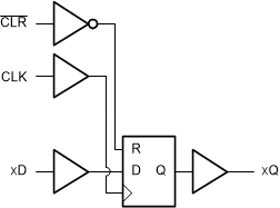
SN74ACT174-Q1 Functional Diagram Functional Diagram