SCAS515G June 1995 – March 2024 SN54ACT240 , SN74ACT240
PRODMIX
- 1
- 1 Features
- 2 Applications
- 3 Description
- 4 Pin Configuration and Functions
- 5 Specifications
- 6 Parameter Measurement Information
- 7 Detailed Description
- 8 Device and Documentation Support
- 9 Revision History
- 10Mechanical, Packaging, and Orderable Information
Package Options
Refer to the PDF data sheet for device specific package drawings
Mechanical Data (Package|Pins)
- DB|20
- RKS|20
- NS|20
- N|20
- DGS|20
- DW|20
- PW|20
Thermal pad, mechanical data (Package|Pins)
- RKS|20
Orderable Information
4 Pin Configuration and Functions
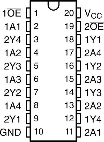
 Figure 4-1 SN54ACT240
J or W Package; SN74ACT240 DB, DGS, DW, N, NS, or PW
Package, (Top View)
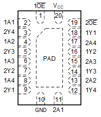
 Figure 4-3 SNx4ACT240
VQFN Package (Top View)
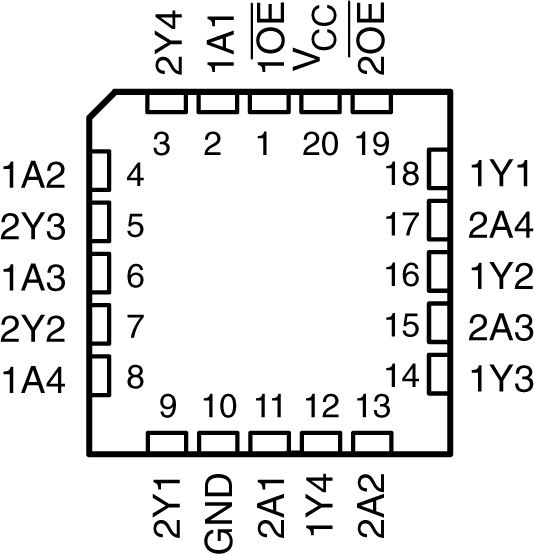
 Figure 4-2 SN54ACT240
FK Package (Top View)
Figure 4-2 SN54ACT240
FK Package (Top View)Table 4-1 Pin Functions
| PIN | TYPE(1) | DESCRIPTION | |
|---|---|---|---|
| NAME | NO. | ||
| 1OE | 1 | I | Output enable 1 |
| 1A1 | 2 | I | 1A1 input |
| 2Y4 | 3 | O | 2Y4 output |
| 1A2 | 4 | I | 1A2 input |
| 2Y3 | 5 | O | 2Y3 output |
| 1A3 | 6 | I | 1A3 input |
| 2Y2 | 7 | O | 2Y2 output |
| 1A4 | 8 | I | 1A4 input |
| 2Y1 | 9 | O | 2Y1 output |
| GND | 10 | — | Ground pin |
| 2A1 | 11 |
I |
2A1 input |
| 1Y4 | 12 | O | 1Y4 output |
| 2A2 | 13 |
I |
2A2 input |
| 1Y3 | 14 | O | 1Y3 output |
| 2A3 | 15 | I | 2A3 input |
| 1Y2 | 16 | O | 1Y2 output |
| 2A4 | 17 | I | 2A4 input |
| 1Y1 | 18 | O | 1Y1 output |
| 2OE | 19 | I | Output enable 2 |
| VCC | 20 | — | Power pin |
| Thermal pad(2) | — | The thermal pad can be connect to GND or left floating. Do not connect to any other signal or supply. | |
(1) Signal Types: I = Input, O = Output, I/O = Input or Output
(2) RKS package only