SCAS517G June 1995 – March 2024 SN54ACT244 , SN74ACT244
PRODUCTION DATA
- 1
- 1 Features
- 2 Applications
- 3 Description
- 4 Pin Configuration and Functions
- 5 Specifications
- 6 Parameter Measurement Information
- 7 Detailed Description
- 8 Application and Implementation
- 9 Device and Documentation Support
- 10Revision History
- 11Mechanical, Packaging, and Orderable Information
Package Options
Refer to the PDF data sheet for device specific package drawings
Mechanical Data (Package|Pins)
- DB|20
- RKS|20
- NS|20
- N|20
- DGS|20
- DW|20
- PW|20
Thermal pad, mechanical data (Package|Pins)
- RKS|20
Orderable Information
4 Pin Configuration and Functions
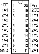
 Figure 4-1 SN54ACT244: J or W Packages,20-Pin CDIP or CFP(Top View)
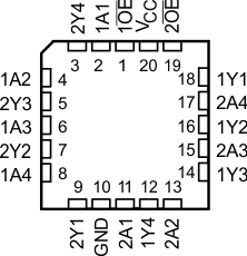
 Figure 4-3 SN54ACT244: FK Package20-Pin LCCC(Top View)
 Figure 4-2 SN74ACT244: DGS, DB, DW, N, NS, or PW
Packages,20-Pin VSSOP SSOP, SOIC,
PDIP, SO, or TSSOP(Top
View)
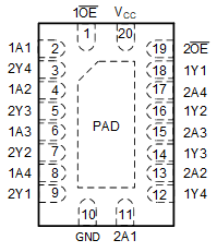
 Figure 4-4 SN74ACT244: RKS Packages,20-Pin VQFN(Top View)
Table 4-1 Pin Functions
| PIN | TYPE(1) | DESCRIPTION | |
|---|---|---|---|
| NO. | NAME | ||
| 1 | 1 OE | I | 1 Active low Output enable |
| 2 | 1A1 | I | 1A1 input |
| 3 | 2Y4 | O | 2Y4 output |
| 4 | 1A2 | I | 1A2 input |
| 5 | 2Y3 | O | 2Y3 Output |
| 6 | 1A3 | I | 1A3 input |
| 7 | 2Y2 | O | 2Y2 Output |
| 8 | 1A4 | I | 1A4 input |
| 9 | 2Y1 | O | 2Y1 Output |
| 10 | GND | — | Ground |
| 11 | 2A1 | I | 2A1 input |
| 12 | 1Y4 | O | 1Y4 output |
| 13 | 2A2 | I | 2A2 input |
| 14 | 1Y3 | O | 1Y3 Output |
| 15 | 2A3 | I | 2A3 input |
| 16 | 1Y2 | O | 1Y2 Output |
| 17 | 2A4 | I | 2A4 input |
| 18 | 1Y1 | O | 1Y1 Output |
| 19 | 2 OE | I | 2 Active low Output enable |
| 20 | VCC | — | Power |
(1) I = input, O = output