SCAS539H October   1995  – March 2024 SN54ACT374 , SN74ACT374

PRODUCTION DATA  

  1.   1
  2. Features
  3. Description
  4. Pin Configuration and Functions
  5. Specifications
    1. 4.1 Absolute Maximum Ratings
    2. 4.2 Recommended Operating Conditions
    3. 4.3 Thermal Information
    4. 4.4 Electrical Characteristics
    5. 4.5 Timing Requirements
    6. 4.6 Switching Characteristics
    7. 4.7 Operating Characteristics
  6. Parameter Measurement Information
  7. Detailed Description
    1. 6.1 Overview
    2. 6.2 Functional Block Diagram
    3. 6.3 Device Functional Modes
  8. Application and Implementation
    1. 7.1 Power Supply Recommendations
    2. 7.2 Layout
      1. 7.2.1 Layout Guidelines
      2. 7.2.2 Layout Example
  9. Device and Documentation Support
    1. 8.1 Documentation Support (Analog)
      1. 8.1.1 Related Links
    2. 8.2 Receiving Notification of Documentation Updates
    3. 8.3 Support Resources
    4. 8.4 Trademarks
    5. 8.5 Electrostatic Discharge Caution
    6. 8.6 Glossary
  10. Revision History
  11. 10Mechanical, Packaging, and Orderable Information

Package Options

Refer to the PDF data sheet for device specific package drawings

Mechanical Data (Package|Pins)
  • DB|20
  • NS|20
  • N|20
  • DW|20
  • PW|20
Thermal pad, mechanical data (Package|Pins)
Orderable Information

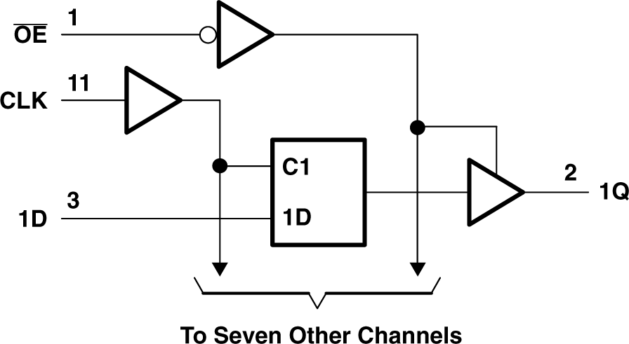
Functional Block Diagram

GUID-185ABD52-6E7A-477B-8295-D197A486EFA8-low.png Figure 6-1 Logic Diagram (Positive Logic)