SCAS538G October 1995 – March 2024 SN54ACT573 , SN74ACT573
PRODUCTION DATA
- 1
- 1 Features
- 2 Applications
- 3 Description
- 4 Pin Configuration and Functions
- 5 Specifications
- 6 Parameter Measurement Information
- 7 Detailed Description
- 8 Application and Implementation
- 9 Device and Documentation Support
- 10Revision History
- 11Mechanical, Packaging, and Orderable Information
Package Options
Refer to the PDF data sheet for device specific package drawings
Mechanical Data (Package|Pins)
- DB|20
- RKS|20
- NS|20
- N|20
- DW|20
- PW|20
Thermal pad, mechanical data (Package|Pins)
- RKS|20
Orderable Information
3 Description
These 8-bit latches feature 3-state outputs designed specifically for driving highly capacitive or relatively low-impedance loads. The devices are particularly suitable for implementing buffer registers, I/O ports, bus drivers, and working registers.
Device Information
| PART NUMBER | RATING | PACKAGE(1) |
|---|---|---|
| SN54ACT573 | Military | J (CDIP, 20) |
| W (CFP, 20) | ||
| FK (LCCC, 20) | ||
| SN74ACT573 | Catalog | DB (SSOP, 20) |
| DW (SOIC, 20) | ||
| N (WQFN, 20) | ||
| NS (SOP, 20) | ||
| PW (TSSOP, 20) | ||
| RKS (VQFN, 20) |
(1) For more information, see Section 11.
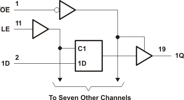
 Logic Diagram (Positive Logic)