SCLS525C July   2003  – April 2024 SN74AHC125-Q1

PRODUCTION DATA  

  1.   1
  2. Features
  3. Applications
  4. Description
  5. Pin Configuration and Functions
  6. Specifications
    1. 5.1 Absolute Maximum Ratings
    2. 5.2 ESD Ratings
    3. 5.3 Recommended Operating Conditions
    4. 5.4 Thermal Information
    5. 5.5 Electrical Characteristics
    6. 5.6 Switching Characteristics, VCC = 3.3 V ± 0.3 V
    7. 5.7 Switching Characteristics, VCC = 5 V ± 0.5 V
    8. 5.8 Noise Characteristics
    9. 5.9 Operating Characteristics
  7. Parameter Measurement Information
  8. Detailed Description
    1. 7.1 Functional Block Diagram
    2. 7.2 Device Functional Modes
  9. Device and Documentation Support
    1. 8.1 Documentation Support
    2. 8.2 Receiving Notification of Documentation Updates
    3. 8.3 Support Resources
    4. 8.4 Trademarks
    5. 8.5 Electrostatic Discharge Caution
    6. 8.6 Glossary
  10. Mechanical, Packaging, and Orderable Information
  11. 10Revision History

Package Options

Refer to the PDF data sheet for device specific package drawings

Mechanical Data (Package|Pins)
  • D|14
  • PW|14
  • BQA|14
Thermal pad, mechanical data (Package|Pins)
Orderable Information

Functional Block Diagram

GUID-887D3341-28F1-47B4-84F3-3EBF8C4B5672-low.png Figure 7-1 Logic Diagram (Positive Logic)
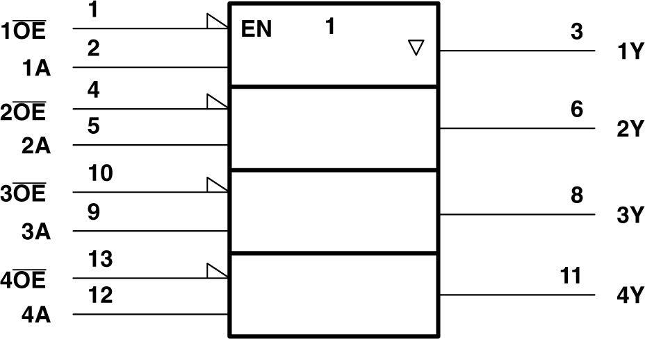
GUID-41293AE6-E46C-4C3D-8070-93C2EB60680B-low.png Figure 7-2 Logic Symbol
(1)
This symbol is in accordance with ANSI/IEEE Std 91-1984 and IEC Publication 617-12.