SCLSA06 February 2024 SN74AHC157-Q1
PRODUCTION DATA
- 1
- 1 Features
- 2 Applications
- 3 Description
- 4 Pin Configuration and Functions
- 5 Specifications
- 6 Parameter Measurement Information
- 7 Detailed Description
- 8 Application and Implementation
- 9 Device and Documentation Support
- 10Revision History
- 11Mechanical, Packaging, and Orderable Information
Package Options
Mechanical Data (Package|Pins)
Thermal pad, mechanical data (Package|Pins)
- BQB|16
Orderable Information
3 Description
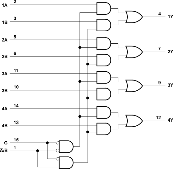
The SN74AHC157-Q1 is a quadruple 2-line to 1-line data selectors/multiplexers are designed for 2-V to 5.5-V VCC operation. The SN74AHC157-Q1 devices feature a common strobe (G) input. When the strobe is high, all outputs are low. When the strobe is low, a 4-bit word is selected from one of two sources and is routed to the four outputs. The device provides true data.
Package
Information
| PART NUMBER | PACKAGE(1) | PACKAGE SIZE(2) | BODY SIZE (NOM)(3) |
|---|---|---|---|
| SN74AHC157-Q1 | BQB (WQFN, 16) | 3.5mm × 2.5mm | 3.5mm × 2.5mm |
| PW (TSSOP, 16) | 5mm × 6.4mm | 5mm × 4.4mm |
(1) For more information, see Section 11.
(2) The package size (length × width) is a nominal value and includes pins, where
applicable
(3) The body size (length × width) is a nominal value and does not include
pins.

Pin numbers shown are for
the D, DB, DGV, J, N, NS, PW, RGY, and W packages.
Logic
Diagram (Positive Logic)