SCLS527E July 2003 – June 2024 SN74AHC245-Q1
PRODUCTION DATA
- 1
- 1 Features
- 2 Applications
- 3 Description
- 4 Pin Configuration and Functions
-
5 Specifications
- 5.1 Absolute Maximum Ratings
- 5.2 ESD Ratings
- 5.3 Recommended Operating Conditions
- 5.4 Thermal Information
- 5.5 Electrical Characteristics
- 5.6 Switching Characteristics, VCC = 3.3 V ± 0.3 V
- 5.7 Switching Characteristics, VCC = 5 V ± 0.5 V
- 5.8 Noise Characteristics
- 5.9 Operating Characteristics
- 5.10 Typical Characteristics
- 6 Parameter Measurement Information
- 7 Detailed Description
- 8 Application and Implementation
- 9 Device and Documentation Support
- 10Revision History
- 11Mechanical, Packaging, and Orderable Information
Package Options
Mechanical Data (Package|Pins)
Thermal pad, mechanical data (Package|Pins)
- RKS|20
Orderable Information
3 Description
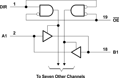
The SN74AHC245-Q1 octal bus transceiver is designed for asynchronous two-way communication between data buses. The control-function implementation minimizes external timing requirements. This device allows data transmission from the A bus to the B bus or from the B bus to the A bus, depending on the logic level at the direction-control (DIR) input. The output-enable (OE) input can be used to disable the device so that the buses effectively are isolated.
To ensure the high-impedance state during power up or power down, OE should be tied to VCC through a pullup resistor; the minimum value of the resistor is determined by the current-sinking capability of the driver.
| PART NUMBER | PACKAGE(1) | PACKAGE SIZE(2) | BODY SIZE(3) |
|---|---|---|---|
| SN74AHC245-Q1 | PW (TSSOP, 20) | 6.50mm × 6.4mm | 6.50mm × 4.40mm |
| RKS (VQFN, 20) | 4.50mm × 2.50mm | 4.50mm × 2.50mm |
 Simplified Schematic