SCLS527E July 2003 – June 2024 SN74AHC245-Q1
PRODUCTION DATA
- 1
- 1 Features
- 2 Applications
- 3 Description
- 4 Pin Configuration and Functions
-
5 Specifications
- 5.1 Absolute Maximum Ratings
- 5.2 ESD Ratings
- 5.3 Recommended Operating Conditions
- 5.4 Thermal Information
- 5.5 Electrical Characteristics
- 5.6 Switching Characteristics, VCC = 3.3 V ± 0.3 V
- 5.7 Switching Characteristics, VCC = 5 V ± 0.5 V
- 5.8 Noise Characteristics
- 5.9 Operating Characteristics
- 5.10 Typical Characteristics
- 6 Parameter Measurement Information
- 7 Detailed Description
- 8 Application and Implementation
- 9 Device and Documentation Support
- 10Revision History
- 11Mechanical, Packaging, and Orderable Information
Package Options
Mechanical Data (Package|Pins)
Thermal pad, mechanical data (Package|Pins)
- RKS|20
Orderable Information
4 Pin Configuration and Functions
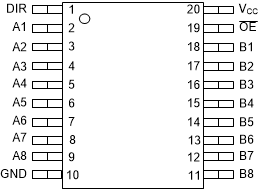
 Figure 4-1 SN74AHC245-Q1 PW Package,20-Pin TSSOP(Top View)
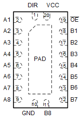
 Figure 4-2 SN74AHC245-Q1 WRKS Package,20-Pin WQFN(Top View)
Table 4-1 Pin Functions
| PIN | TYPE(1) | DESCRIPTION | |
|---|---|---|---|
| NO. | NAME | ||
| 1 | DIR | I/O | Direction control input (L = B → A, H = A → B) |
| 2 | A1 | I/O | Channel 1 output/input A |
| 3 | A2 | I/O | Channel 2 output/input A |
| 4 | A3 | I/O | Channel 3 output/input A |
| 5 | A4 | I/O | Channel 4 output/input A |
| 6 | A5 | I/O | Channel 5 output/input A |
| 7 | A6 | I/O | Channel 6 output/input A |
| 8 | A7 | I/O | Channel 7 output/input A |
| 9 | A8 | I/O | Channel 8 output/input A |
| 10 | GND | G | Ground |
| 11 | B8 | I/O | Channel 8 input/output B |
| 12 | B7 | I/O | Channel 7 input/output B |
| 13 | B6 | I/O | Channel 6input/output B |
| 14 | B5 | I/O | Channel 5input/output B |
| 15 | B4 | I/O | Channel 4input/output B |
| 16 | B3 | I/O | Channel 3input/output B |
| 17 | B2 | I/O | Channel 2input/output B |
| 18 | B1 | I/O | Channel 1input/output B |
| 19 | OE | I/O | Output enable, active low |
| 20 | VCC | P | Positive supply |
| Thermal Pad | — | Thermal Pad(2) | |
(1) I = Input, O = Output, I/O = Input or Output, G = Ground, P = Power.
(2) WRKS Package Only