SCLSA03 March 2024 SN74AHC257
PRODUCTION DATA
- 1
- 1 Features
- 2 Applications
- 3 Description
- 4 Pin Configuration and Functions
- 6
- 7
- 5 Specifications
- 6 Parameter Measurement Information
- 7 Detailed Description
- 8 Application and Implementation
- 9 Device and Documentation Support
- 10Revision History
- 11Mechanical, Packaging, and Orderable Information
Package Options
Refer to the PDF data sheet for device specific package drawings
Mechanical Data (Package|Pins)
- BQB|16
- PW|16
Thermal pad, mechanical data (Package|Pins)
- BQB|16
Orderable Information
6 Parameter Measurement Information
Phase relationships between waveforms were chosen arbitrarily for the examples listed in the following table. All input pulses are supplied by generators having the following characteristics: PRR ≤ 1MHz, ZO = 50Ω, tt < 2ns.
The outputs are measured individually with one input transition per measurement.
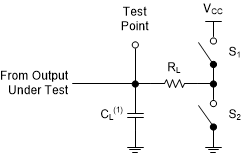
| TEST | S1 | S2 | RL | CL | ΔV | VCC |
|---|---|---|---|---|---|---|
| tPLH, tPHL | OPEN | OPEN | — | 15pF, 50pF | — | ALL |
| tPLZ, tPZL | CLOSED | OPEN | 1kΩ | 15pF, 50pF | 0.15V | ≤ 2.5V |
| tPHZ, tPZH | OPEN | CLOSED | 1kΩ | 15pF, 50pF | 0.15V | ≤ 2.5V |
| tPLZ, tPZL | CLOSED | OPEN | 1kΩ | 15pF, 50pF | 0.3V | > 2.5V |
| tPHZ, tPZH | OPEN | CLOSED | 1kΩ | 15pF, 50pF | 0.3V | > 2.5V |

(1) CL includes probe
and test-fixture capacitance.
Figure 6-1 Load Circuit for 3-State
Outputs
(3) The greater between
tPZL and tPZH is the same as
ten.
(4) The greater between
tPLZ and tPHZ is the same as
tdis.
Figure 6-3 Voltage Waveforms
Propagation Delays
Noise values measured with all
other outputs simultaneously switching.
Figure 6-5 Voltage Waveforms, Noise
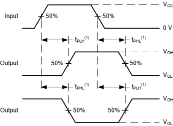
(1) The
greater between tPLH and tPHL is the same as
tpd.
Figure 6-2 Voltage Waveforms
Propagation Delays
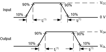
(1) The greater between
tr and tf is the same as tt.
Figure 6-4 Voltage Waveforms, Input
and Output Transition Times