SCLS247L October 1995 – February 2024 SN54AHC32 , SN74AHC32
PRODUCTION DATA
- 1
- 1 Features
- 2 Applications
- 3 Description
- 4 Pin Configuration and Functions
- 5 Specifications
- 6 Parameter Measurement Information
- 7 Detailed Description
- 8 Application and Implementation
- 9 Device and Documentation Support
- 10Revision History
- 11Mechanical, Packaging, and Orderable Information
4 Pin Configuration and Functions
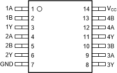
 Figure 4-1 SN54AHC32 J or W
SN74AHC32 D, DB, DGV, N, NS or PW Package, 14-Pin (Top View)
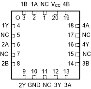
 Figure 4-3 SN54AHC32 FK Package, 20-Pin (Top View)
 Figure 4-2 SN74AHC32 RGY or BQA Package, 14-Pin (Top View)
Table 4-1 Pin Functions
| PIN | TYPE(1) | DESCRIPTION | |||
|---|---|---|---|---|---|
| NAME | SN74AHC32 | SN54AHC32 | |||
| D, DB, DGV, N, NS, PW, RGY, BQA | J, W | FK | |||
| 1A | 1 | 1 | 2 | I | 1A Input |
| 1B | 2 | 23 | 3 | I | 1B Input |
| 1Y | 3 | 3 | 4 | O | 1Y Output |
| 2A | 4 | 4 | 6 | I | 2A Input |
| 2B | 5 | 5 | 8 | I | 2B Input |
| 2Y | 6 | 6 | 9 | O | 2Y Output |
| 3A | 9 | 9 | 13 | I | 3A Input |
| 3B | 10 | 10 | 14 | I | 3B Input |
| 3Y | 8 | 8 | 12 | O | 3Y Output |
| 4A | 12 | 12 | 18 | I | 4A Input |
| 4B | 13 | 13 | 19 | I | 4B Input |
| 4Y | 11 | 11 | 16 | O | 4Y Output |
| GND | 7 | 7 | 10 | — | Ground Pin |
| NC | — | — | 1, 5, 7, 11, 15, 17 | — | No Connection |
| VCC | 14 | 14 | 20 | — | Power Pin |
Thermal Pad(2) | – | – | – | – | Thermal Pad |
(1) Signal Types: I = Input, O = Output, I/O = Input or Output.
(2) RGY and BQA Package Only