SCLS603C December 2004 – July 2024 SN74AHC541-Q1
PRODMIX
- 1
- 1 Features
- 2 Applications
- 3 Description
- 4 Pin Configuration and Functions
- 5 Specifications
- 6 Parameter Measurement Information
- 7 Detailed Description
- 8 Application and Implementation
- 9 Device and Documentation Support
- 10Revision History
- 11Mechanical, Packaging, and Orderable Information
Package Options
Refer to the PDF data sheet for device specific package drawings
Mechanical Data (Package|Pins)
- PW|20
Thermal pad, mechanical data (Package|Pins)
Orderable Information
3 Description
The SN74AHC541 octal buffer/driver is
ideal for driving bus lines or buffer memory address registers. This device features
inputs and outputs on opposite sides of the package to facilitate printed circuit board
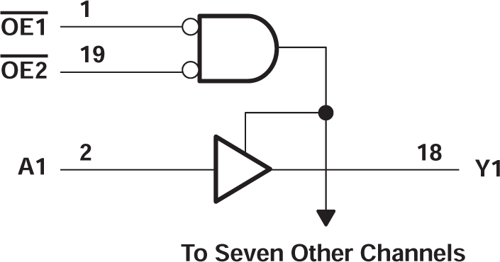
layout. Logic Diagram (Positive Logic)
Package Information
| PART NUMBER | PACKAGE(1) | PACKAGE SIZE(2) | BODY SIZE(3) |
|---|---|---|---|
| SN74AHC541-Q1 | PW (TSSOP, 20) | 6.5mm × 6.4mm | 6.5mm × 4.4mm |
(1) For more information, see Section 11.
(2) The package size (length × width)
is a nominal value and includes pins, where applicable.
(3) The body size (length × width) is
a nominal value and does not include pins.
 Logic Diagram (Positive Logic)