SCLS261P October 1995 – August 2024 SN54AHC541 , SN74AHC541
PRODUCTION DATA
- 1
- 1 Features
- 2 Applications
- 3 Description
- 4 Pin Configuration and Functions
-
5 Specifications
- 5.1 Absolute Maximum Ratings
- 5.2 ESD Ratings
- 5.3 Recommended Operating Conditions
- 5.4 Thermal Information
- 5.5 Electrical Characteristics
- 5.6 Switching Characteristics, VCC = 3.3 V ± 0.3 V
- 5.7 Switching Characteristics, VCC = 5 V ± 0.5 V
- 5.8 Noise Characteristics
- 5.9 Operating Characteristics
- 5.10 Typical Characteristics
- 6 Parameter Measurement Information
- 7 Detailed Description
- 8 Application and Implementation
- 9 Device and Documentation Support
- 10Revision History
- 11Mechanical, Packaging, and Orderable Information
Package Options
Refer to the PDF data sheet for device specific package drawings
Mechanical Data (Package|Pins)
- DGV|20
- DB|20
- NS|20
- N|20
- DW|20
- PW|20
Thermal pad, mechanical data (Package|Pins)
Orderable Information
3 Description
The SNx4AHC541 octal buffers and drivers are ideal for driving bus lines or buffer memory address registers. These devices feature inputs and outputs on opposite sides of the package to facilitate printed circuit board layout.
Device Information
| PART NUMBER | PACKAGE(1) | PACKAGE SIZE(2) | BODY SIZE(3) |
|---|---|---|---|
| SNx4AHC541 | N (PDIP, 20) | 24.33mm x 9.4mm | 25.40mm x 6.35mm |
| NS (SOP, 20) | 12.6mm x 7.8mm | 12.6mm x 5.3mm | |
| DB (SSOP, 20) | 7.2mm × 7.8mm | 7.50mm x 5.30mm | |
| PW (TSSOP, 20) | 6.50mm × 6.4mm | 6.50mm x 4.40mm | |
| DGV (TVSOP, 20) | 5.00mm x 6.4mm | 5.00mm x 4.40mm | |
| DW (SOIC, 20) | 12.80mm × 10.3mm | 12.80mm x 7.50mm | |
| J (CDIP, 20) | 24.2mm x 7.62mm | 24.2mm x 6.92mm | |
| W (CFP, 20) | 13.09mm x 8.13mm | 13.09mm x 6.92mm | |
| FK (LCCC, 20) | 8.89mm x 8.89mm | 8.89mm x 8.89mm |
(1) For more information, see Section 11.
(2) The package size (length × width)
is a nominal value and includes pins, where applicable.
(3) The body size (length × width) is
a nominal value and does not include pins.
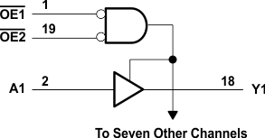
 Simplified Block Diagram