SCAS998 March 2024 SN74AHC594-Q1
PRODUCTION DATA
- 1
- 1 Features
- 2 Applications
- 3 Description
- 4 Pin Configuration and Functions
- 5 Specifications
- 6 Parameter Measurement Information
- 7 Detailed Description
- 8 Application and Implementation
- 9 Device and Documentation Support
- 10Revision History
- 11Mechanical, Packaging, and Orderable Information
Package Options
Mechanical Data (Package|Pins)
Thermal pad, mechanical data (Package|Pins)
- BQB|16
Orderable Information
3 Description
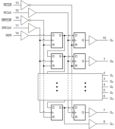
The SN74AHC594-Q1 is an 8-bit serial-in, parallel-out shift register that feeds an 8-bit D-type storage register. Separate clocks (RCLK, SRCLK) and direct overriding clear (RCLR, SRCLR) inputs are provided on both the shift and storage registers. A serial (QH') output is provided for cascading purposes.
Both the shift register (SRCLK) and storage register (RCLK) clocks are positive edge triggered. If both clocks are connected together, the shift register always is one clock pulse ahead of the storage register.
Package
Information
| PART NUMBER | PACKAGE(1) | PACKAGE SIZE(2) | BODY SIZE (NOM)(3) |
|---|---|---|---|
| SN74AHC594-Q1 | WBQB (WQFN, 16) | 3.5mm × 2.5mm | 3.5mm × 2.5mm |
| PW (TSSOP, 16) | 5mm × 6.4mm | 5mm × 4.4mm |
(1) For more information, see Section 11.
(2) The package size (length × width) is a nominal value and includes pins, where
applicable
(3) The body size (length × width) is a nominal value and does not include
pins.
 Logic
Diagram (Positive Logic)