SCLS537E August 2003 – April 2024 SN74AHC595-Q1
PRODMIX
- 1
- 1 Features
- 2 Applications
- 3 Description
- 4 Pin Configuration and Functions
-
5 Specifications
- 5.1 Absolute Maximum Ratings
- 5.2 Recommended Operating Conditions
- 5.3 Thermal Information
- 5.4 Electrical Characteristics
- 5.5 Timing Requirements, VCC = 3.3 V ± 0.3 V
- 5.6 Timing Requirements, VCC = 5 V ± 0.5 V
- 5.7 Timing Diagrams
- 5.8 Switching Characteristics, VCC = 3.3 V ± 0.3 V
- 5.9 Switching Characteristics, VCC = 5 V ± 0.5 V
- 6 Parameter Measurement Information
- 7 Detailed Description
- 8 Application and Implementation
- 9 Device and Documentation Support
- 10Revision History
- 11Mechanical, Packaging, and Orderable Information
Package Options
Refer to the PDF data sheet for device specific package drawings
Mechanical Data (Package|Pins)
- PW|16
- BQB|16
Thermal pad, mechanical data (Package|Pins)
- BQB|16
Orderable Information
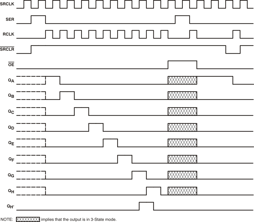
5.7 Timing Diagrams
