SGDS020D February 2002 – February 2024 SN74AHC74Q-Q1
PRODUCTION DATA
- 1
- 1 Features
- 2 Applications
- 3 Description
- 4 Pin Configuration and Functions
-
5 Specifications
- 5.1 Absolute Maximum Ratings
- 5.2 ESD Ratings
- 5.3 Recommended Operating Conditions
- 5.4 Thermal Information — SN74AHC74Q-Q1
- 5.5 Electrical Characteristics
- 5.6 Timing Requirements — VCC = 3.3 V ± 0.3 V
- 5.7 Timing Requirements — VCC = 5 V ± 0.5 V
- 5.8 Switching Characteristics, VCC = 3.3 V ± 0.3 V
- 5.9 Switching Characteristics, VCC = 5 V ± 0.5 V
- 5.10 Noise Characteristics
- 5.11 Operating Characteristics
- 5.12 Typical Characteristics
- 6 Parameter Measurement Information
- 7 Detailed Description
- 8 Application and Implementation
- 9 Device and Documentation Support
- 10Revision History
- 11Mechanical, Packaging, and Orderable Information
Package Options
Refer to the PDF data sheet for device specific package drawings
Mechanical Data (Package|Pins)
- D|14
- PW|14
- BQA|14
Thermal pad, mechanical data (Package|Pins)
- BQA|14
Orderable Information
4 Pin Configuration and Functions
 Figure 4-1 SN74AHC74Q-Q1
D or PW Package, 14-Pin SOIC or TSSOP (Top View)
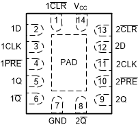
 Figure 4-2 SN74AHC74Q-Q1
BQA Package, 14-Pin WQFN (Transparent Top View)
Figure 4-2 SN74AHC74Q-Q1
BQA Package, 14-Pin WQFN (Transparent Top View)Table 4-1 Pin Functions
| PIN | TYPE(1) | DESCRIPTION | |
|---|---|---|---|
| NAME | NO. | ||
| 1CLR | 1 | I | Asynchronous clear for channel 1, active low |
| 1D | 2 | I | Data for channel 1 |
| 1CLK | 3 | I | Clock for channel 1, rising edge triggered |
| 1PRE | 4 | I | Asynchronous preset for channel 1, active low |
| 1Q | 5 | O | Output for channel 1 |
| 1Q | 6 | O | Inverted output for channel 1 |
| GND | 7 | G | Ground |
| 2Q | 8 | O | Inverted output for channel 2 |
| 2Q | 9 | O | Output for channel 2 |
| 2PRE | 10 | I | Asynchronous preset for channel 2, active low |
| 2CLK | 11 | I | Clock for channel 2, rising edge triggered |
| 2D | 12 | I | Data for channel 2 |
| 2CLR | 13 | I | Asynchronous clear for channel 2, active low |
| VCC | 14 | P | Positive supply |
| Thermal Pad(2) | — | The thermal pad can be connected to GND or left floating. Do not connect to any other signal or supply | |
(1) I = input, O = output, P = power, G = ground
(2) BQA package only