SCLS508C June 2003 – October 2023 SN74AHCT125-Q1
PRODUCTION DATA
- 1
- 1 Features
- 2 Applications
- 3 Description
- 4 Revision History
- 5 Pin Configuration and Functions
-
6 Specifications
- 6.1 Absolute Maximum Ratings
- 6.2 ESD Ratings
- 6.3 Recommended Operating Conditions
- 6.4 Thermal Information
- 6.5 Electrical Characteristics
- 6.6 Switching Characteristics
- 6.7 Noise Characteristics #GUID-59737337-6F0E-416E-BD36-E176D00EBAF4/SCLS5085302
- 6.8 Operating Characteristics
- 6.9 Typical Characteristics
- 7 Parameter Measurement Information
- 8 Detailed Description
- 9 Application and Implementation
- 10Device and Documentation Support
- 11Mechanical, Packaging, and Orderable Information
Package Options
Mechanical Data (Package|Pins)
Thermal pad, mechanical data (Package|Pins)
- BQA|14
Orderable Information
3 Description
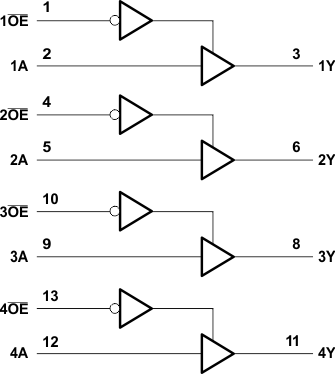
The SN74AHCT125-Q1 devices are quadruple bus buffer gates featuring independent line drivers with 3-state outputs. Each output is disabled when the associated output-enable (OE) input is high. When OE is low, the respective gate passes the data from the A input to its Y output.
To ensure the high-impedance state during power up or power down, OE should be tied to VCC through a pullup resistor; the minimum value of the resistor is determined by the current-sinking capability of the driver.
Package Information
| PART NUMBER | PACKAGE(1) | PACKAGE SIZE(2) |
|---|---|---|
| SN74AHCT125-Q1 | D (SOIC, 14) | 8.65 mm 6 mm |
| PW (TSSOP, 14) | 5 mm 6.4 mm | |
| BQA (TSSOP, 14) | 3 mm 2.5 mm |
(1) For all available packages, see the orderable addendum at the end of the data sheet.
(2) The package size (length × width) is a nominal value and includes pins, where applicable.
 Logic Diagram (Positive Logic)