SGDS024A february 2002 – may 2023 SN74AHCT244Q
PRODMIX
- 1
- 1Features
- 2Description
- 3Revision History
- 4Pin Configuration and Functions
- 5Specifications
- 6Parameter Measurement Information
- 7Detailed Description
Package Options
Refer to the PDF data sheet for device specific package drawings
Mechanical Data (Package|Pins)
- DW|20
- PW|20
Thermal pad, mechanical data (Package|Pins)
Orderable Information
4 Pin Configuration and Functions
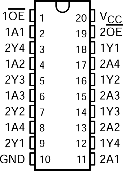
 Figure 4-1 DW or PW Package (Top
View)
Figure 4-1 DW or PW Package (Top
View)Pin Functions
| PIN | I/O1 | DESCRIPTION | |
|---|---|---|---|
| Name | NO. | ||
| 1OE | 1 | I | Bank 1, output enable, active low |
| 1A1 | 2 | I | Bank 1, channel 1 input |
| 2Y4 | 3 | O | Bank 2, channel 4 output |
| 1A2 | 4 | I | Bank 1, channel 2 input |
| 2Y3 | 5 | O | Bank 2, channel 3 output |
| 1A3 | 6 | I | Bank 1, channel 3 input |
| 2Y2 | 7 | O | Bank 2, channel 2 output |
| 1A4 | 8 | I | Bank 1, channel 4 input |
| 2Y1 | 9 | O | Bank 2, channel 1 output |
| GND | 10 | — | Ground |
| 2A1 | 11 | I | Bank 2, channel 1 input |
| 1Y4 | 12 | O | Bank 1, channel 4 output |
| 2A2 | 13 | I | Bank 2, channel 2 input |
| 1Y3 | 14 | O | Bank 1, channel 3 output |
| 2A3 | 15 | I | Bank 2, channel 3 input |
| 1Y2 | 16 | O | Bank 1, channel 2 output |
| 2A4 | 17 | I | Bank 2, channel 4 input |
| 1Y1 | 18 | O | Bank 1, channel 1 output |
| 2OE | 19 | I | Bank 2, output enable, active low |
| VCC | 20 | — | Positive supply |