SCLS910 April 2023 SN74AHCT245-Q1
PRODUCTION DATA
- 1 Features
- 2 Applications
- 3 Description
- 4 Revision History
- 5 Pin Configuration and Functions
- 6 Specifications
- 7 Parameter Measurement Information
- 8 Detailed Description
- 9 Application and Implementation
- 10Power Supply Recommendations
- 11Layout
- 12Device and Documentation Support
- 13Mechanical, Packaging, and Orderable Information
Package Options
Mechanical Data (Package|Pins)
- PW|20
Thermal pad, mechanical data (Package|Pins)
Orderable Information
3 Description
The SN74AHCT245-Q1 octal bus transceivers are designed for asynchronous two-way communication between data buses. These parts operate from 4.5 V to 5.5 V.
Package Information(1)
| PART NUMBER | PACKAGE | BODY SIZE (NOM) |
|---|---|---|
| SN74AHCT245-Q1 | PW (TSSOP, 20) | 6.50 mm × 4.40 mm |
(1) For all available packages, see the orderable addendum at the end of the data sheet.
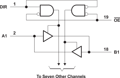
 Simplified Schematic