SCLS241N October 1995 – August 2024 SN54AHCT374 , SN74AHCT374
PRODMIX
- 1
- 1 Features
- 2 Applications
- 3 Description
- 4 Pin Configuration and Functions
- 5 Specifications
- 6 Parameter Measurement Information
- 7 Detailed Description
- 8 Application and Implementation
- 9 Device and Documentation Support
- 10Revision History
- 11Mechanical, Packaging, and Orderable Information
Package Options
Refer to the PDF data sheet for device specific package drawings
Mechanical Data (Package|Pins)
- DB|20
- N|20
- DW|20
- PW|20
Thermal pad, mechanical data (Package|Pins)
Orderable Information
3 Description
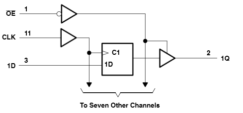
The 'AHCT374 devices are octal edge-triggered D-type flip-flops that feature 3-state outputs designed specifically for driving highly capacitive or relatively low-impedance loads. This device is particularly suitable for implementing buffer registers, I/O ports, bidirectional bus drivers, and working registers.
On the positive transition of the clock (CLK) input, the Q outputs are set to the logic levels of the data (D) inputs.
Device Information
| PART NUMBER | PACKAGE(1) | PACKAGE SIZE(2) | BODY SIZE(3) |
|---|---|---|---|
| SNx4AHCT374 | DB (SSOP, 20) | 7.2mm × 7.8mm | 7.50mm x 5.30mm |
| DW (SOIC, 20) | 12.80mm × 10.3mm | 12.8mm x 7.5mm | |
| N (PDIP, 20) | 24.33mm x 9.4mm | 25.40mm x 6.35mm | |
| PW (TSSOP, 20) | 6.50mm × 6.4mm | 6.50mm x 4.40mm | |
| J (CDIP, 20) | 24.2mm x 7.62mm | 24.2mm x 6.92mm | |
| W (CFP, 20) | 13.09mm x 8.13mm | 13.09mm x 6.92mm | |
| FK (LCCC, 20) | 8.89mm x 8.89mm | 8.89mm x 8.89mm |
(1) For more information, see Section 11.
(2) The package size (length × width)
is a nominal value and includes pins, where applicable.
(3) The body size (length × width) is
a nominal value and does not include pins.
 Logic Diagram (Positive Logic)